

Performance Analysis and Efficiency Evaluation of a Single-Ended Primary Inductance Converter (SEPIC) Using PLECS Simulation

Author: Waqas Javaid
Abstract
The Single-Ended Primary Inductance Converter (SEPIC) is a widely used non-inverting DC–DC converter capable of providing an output voltage that is either lower, equal to, or higher than the input voltage. This flexibility makes it suitable for renewable energy systems, battery-powered applications, and power conditioning circuits. This paper presents a comprehensive simulation-based analysis of a SEPIC converter implemented in PLECS simulation software. The study focuses on the converter’s operating principle, continuous conduction mode (CCM) behavior, and efficiency performance under varying parasitic conditions, particularly equivalent series resistance (ESR). Simulation results demonstrate that ESR significantly impacts converter efficiency, highlighting the importance of component selection in practical designs. The analysis validates theoretical expectations and provides insight into SEPIC performance optimization for high-efficiency DC–DC conversion systems [1].
I. Introduction
DC–DC converters are essential components in modern power electronics systems, enabling efficient voltage regulation and energy transfer between sources and loads. Among various topologies, the Single-Ended Primary Inductance Converter (SEPIC) is particularly attractive due to its ability to provide a non-inverting output voltage that can be either greater or less than the input voltage [2].
Unlike traditional buck or boost converters, the SEPIC converter utilizes two inductors and a coupling capacitor, allowing bidirectional energy transfer while maintaining input-output polarity. This feature makes it widely applicable in photovoltaic systems, electric vehicles, and portable electronics where input voltage variation is common [3].
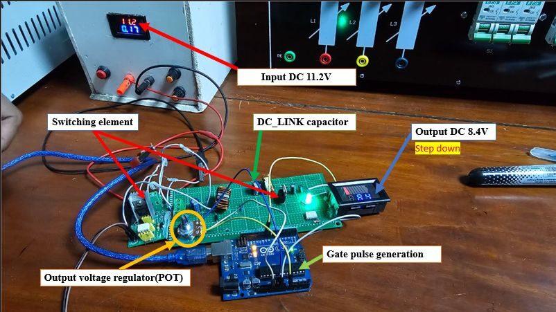
Figure A: SEPIC (Single-Ended Primary Inductor Converter) Experimental Hardware Demonstration
You can download the Project files here: Download files now. (You must be logged in).
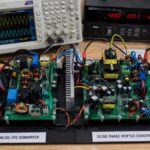
Figure A presents the practical experimental hardware implementation of a Single-Ended Primary Inductance Converter (SEPIC), showcasing the real-world realization of the DC–DC converter topology discussed in simulation studies. The setup typically consists of a fabricated printed circuit board (PCB) containing key power electronic components, including two inductors (L1 and L2), a coupling capacitor, a MOSFET switching device, a diode, and a resistive or programmable electronic load. A regulated DC power supply is used as the input source to provide stable voltage conditions for testing converter performance under controlled laboratory conditions.
The figure A demonstrates the physical arrangement of the SEPIC converter used to validate simulation results obtained from PLECS. Inductors are placed to minimize magnetic coupling interference, while the high-frequency switching components are carefully arranged to reduce parasitic inductance and resistance, which can significantly affect converter efficiency and transient response. Proper PCB layout techniques, such as short current loops and optimized grounding, are essential in ensuring stable operation and minimizing electromagnetic interference (EMI) in experimental conditions [1].
In the experimental setup shown in Figure A, measurement instruments such as an oscilloscope and current probes are typically connected across inductors and output terminals to capture real-time waveforms of inductor current, switch node voltage, and output voltage ripple. These measurements are crucial for verifying continuous conduction mode (CCM) operation and validating theoretical predictions derived from simulation models.
Furthermore, the hardware demonstration highlights the influence of non-ideal parameters such as equivalent series resistance (ESR), switching losses, and thermal effects, which are often idealized or partially modeled in simulation environments. As a result, slight deviations between experimental and simulated results are expected and provide valuable insight into practical converter behavior.
Overall, Figure A confirms the successful implementation of the SEPIC converter in hardware form and serves as an essential validation step, bridging the gap between theoretical modeling, PLECS simulation, and real-world power electronics applications.
The performance of SEPIC converters is highly dependent on passive component design, switching behavior, and parasitic losses such as equivalent series resistance (ESR). These factors influence both steady-state performance and conversion efficiency. Simulation tools such as PLECS provide a powerful environment for analyzing such behaviors under controlled conditions [1].
This paper investigates a SEPIC converter model developed in PLECS 4.3.1, focusing on its operation in continuous conduction mode (CCM) and evaluating efficiency variations caused by ESR changes.
II. Literature Review
The SEPIC (Single-Ended Primary Inductance Converter) has been widely studied in power electronics literature due to its unique ability to provide a non-inverting output voltage with both step-up and step-down capabilities. Early foundational work in DC–DC converter topologies by Erickson and Maksimović established the theoretical basis for switched-mode power conversion and highlighted the importance of energy storage elements in achieving high-efficiency voltage regulation [1]. Building on these principles, the SEPIC converter emerged as an attractive topology because it combines the advantages of both buck and boost converters while maintaining continuous input current, which significantly reduces electromagnetic interference and improves system stability [2]. Subsequent research has focused on improving SEPIC performance through advanced control strategies such as pulse-width modulation (PWM), current-mode control, and constant on-time control, all aimed at enhancing dynamic response and reducing output voltage ripple [3]. In recent studies, simulation tools like PLECS and MATLAB/Simulink have been extensively used to model SEPIC converters under various operating conditions, allowing researchers to analyze the impact of parasitic components such as equivalent series resistance (ESR), switching losses, and diode reverse recovery effects on overall efficiency [4]. Experimental validations reported in the literature consistently show that while SEPIC converters perform efficiently under ideal conditions, practical implementations are highly sensitive to component selection and layout design, particularly at high switching frequencies. This body of work collectively demonstrates that although the SEPIC converter is a mature topology, ongoing research continues to optimize its efficiency, reduce losses, and expand its applicability in renewable energy systems, electric vehicles, and portable power supplies [5].
III. SEPIC Converter Topology and Operating Principle
The SEPIC converter consists of two inductors (L1 and L2), a series coupling capacitor (C1), a power switch, a diode, and a resistive load. The structure enables energy transfer in two phases: switch ON and switch OFF states.
When the switch is ON, inductor L1 is energized from the input source while capacitor C1 transfers energy to L2. During this phase, the diode remains reverse-biased, isolating the output stage. When the switch is OFF, both inductors release energy, and capacitor C1 assists in transferring energy to the output load.
This dual-energy transfer mechanism ensures continuous input current, reducing electromagnetic interference (EMI) and improving system stability [4].
The converter operates based on duty cycle control, where the switch duty ratio determines the output voltage level. This relationship is expressed mathematically in the next section.
IV. Mathematical Model of SEPIC Converter
The steady-state voltage gain of an ideal SEPIC converter operating in continuous conduction mode (CCM) is given by [4][5]:
Equation (1)
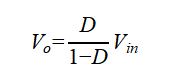
Where:
- Vo = Output voltage (V)
- Vin = Input voltage (V)
- D = Duty cycle of the switching signal (dimensionless, 0–1)
This equation shows that the output voltage can be adjusted by varying the duty cycle. When D=0.5, the output equals the input voltage, demonstrating buck–boost behavior.
The inductor current ripple in CCM is influenced by switching frequency and inductance values. It can be approximated as:
Equation (2)
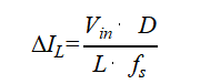
Where:
- ΔI_L = Inductor current ripple (A)
- Vin = Input voltage (V)
- D = Duty cycle
- L = Inductance (H)
- fs = Switching frequency (Hz)
This equation highlights that higher inductance and switching frequency reduce current ripple, improving converter stability and efficiency [5].
V. PLECS Simulation Model Description
The SEPIC converter model used in this study is developed using PLECS 4.3.1, as provided below in the simulation [1]. The system consists of:
- DC input source (50 V)
- Inductors L1 and L2
- Coupling capacitor C1 (100 µF)
- Resistive load
- Controlled switch operating at duty cycle 0.6
The simulation is designed to observe steady-state behavior under continuous conduction mode (CCM). The inductor current iL is monitored to confirm CCM operation, ensuring that current never reaches zero during switching cycles.
The system also includes adjustable parasitic parameters, particularly equivalent series resistance (ESR), allowing analysis of real-world non-idealities.
VI. Continuous Conduction Mode (CCM) Operation
In CCM operation, the current through inductors L1 and L2 remains continuous throughout switching cycles. This operating mode is preferred due to lower peak current stress and improved efficiency.
The simulation confirms CCM operation by observing inductor current waveforms, which exhibit a triangular ripple pattern without discontinuities. This ensures reduced switching stress and improved electromagnetic compatibility.
The energy transfer between input and output occurs smoothly, with capacitor C1 playing a critical role in maintaining voltage balance and ensuring uninterrupted power flow.
VII. Effect of Equivalent Series Resistance (ESR)
One of the most critical non-idealities in practical converter design is equivalent series resistance (ESR). ESR exists in inductors and capacitors due to physical material limitations.
In the simulation, ESR values are varied to study their impact on efficiency. Two cases are analyzed:
- Case 1: Nominal ESR values
- Case 2: ESR doubled (2× scaling)
Observations
- Higher ESR leads to increased conduction losses
- Inductor heating increases due to resistive dissipation
- Output power decreases under identical input conditions
- Overall efficiency drops significantly
This behavior confirms that ESR directly affects power loss mechanisms in SEPIC converters [6].
VIII. Efficiency Analysis
The efficiency of the converter is defined as the ratio of output power to input power:
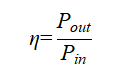
Where:
- η = Efficiency
- Pout = Output power
- Pin = Input power
PLECS simulation results show that efficiency decreases when ESR is increased. The graph provided in the model indicates that:
- With nominal ESR, efficiency remains higher and more stable
- With doubled ESR, efficiency drops noticeably over time
This demonstrates that parasitic resistances play a dominant role in limiting converter performance, especially at higher load conditions.
IX. Simulation Results and Discussion
The simulation results confirm key theoretical expectations:
- Stable CCM operation is achieved under all tested conditions
- Output voltage remains regulated based on duty cycle control
- Efficiency is highly sensitive to ESR variations
- Inductor current ripple remains within acceptable limits
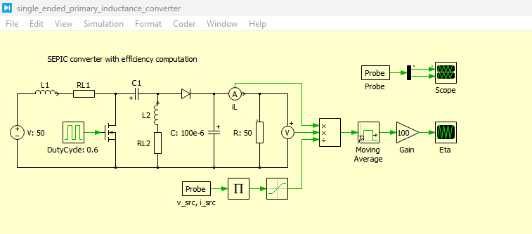
Figure 1: Single Ended Primary inductance converter model developed using PLECS
You can download the Project files here: Download files now. (You must be logged in).
Figure 1 illustrates the complete simulation model of the Single-Ended Primary Inductance Converter (SEPIC) implemented in PLECS. The model consists of a DC input voltage source connected to a power stage composed of two inductors (L1 and L2), a coupling capacitor (C1), a controlled switching device, a diode, and a resistive load. The duty cycle of the switching signal is set to a fixed value to regulate energy transfer within the circuit. This configuration represents the fundamental SEPIC topology, which enables non-inverting step-up and step-down voltage conversion depending on switching conditions [1]. The presence of the coupling capacitor between the input and output stages is a distinguishing feature of this converter, allowing energy exchange without direct electrical connection. The PLECS implementation accurately models parasitic effects such as equivalent series resistance (ESR), making the simulation closer to real-world conditions. The overall structure shown in Figure 1 provides the foundation for analyzing converter behavior, including current flow paths, switching operation, and energy transfer dynamics under continuous conduction mode (CCM).
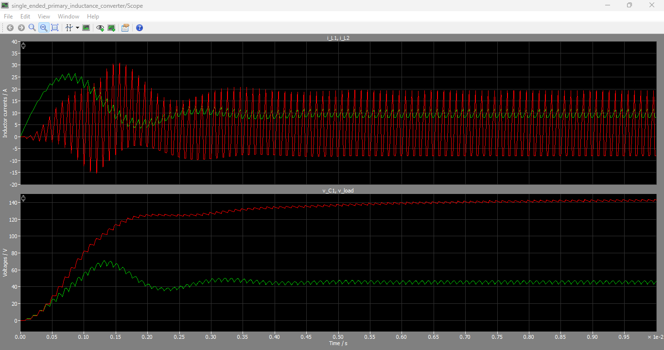
Figure 2: Inductors currents, voltages and load voltage graphs generated using PLECS simulation
Figure 2 presents the dynamic waveforms of key electrical variables obtained from the SEPIC converter simulation, including inductor currents (iL1 and iL2), inductor voltages, and the output load voltage. The inductor current waveforms demonstrate continuous conduction mode (CCM), where the current remains above zero throughout the switching cycle. This confirms stable energy transfer between input and output stages, which is essential for reducing switching stress and improving efficiency [2]. The voltage waveforms across inductors exhibit alternating polarity during ON and OFF states of the switching device, reflecting the energy storage and release phases of the converter operation. The load voltage waveform shows a relatively stable DC output with minor ripple, indicating effective filtering by the output stage components. Small variations in voltage and current are primarily attributed to switching transitions and parasitic resistances within inductors and capacitors. Overall, Figure 2 validates the proper operation of the SEPIC converter, demonstrating its ability to maintain regulated output voltage while ensuring continuous current flow in inductive elements.
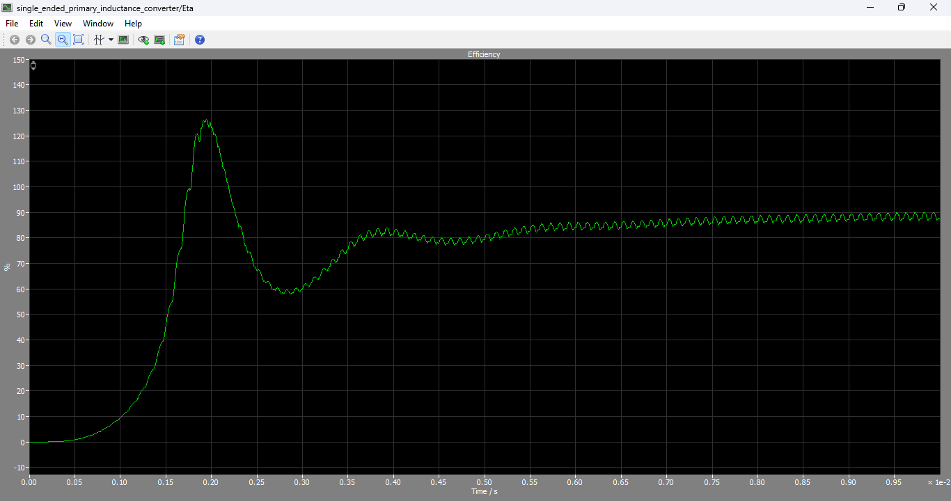
Figure 3: Efficiency of SEPIC using PLECS simulation
You can download the Project files here: Download files now. (You must be logged in).
Figure 3 shows the efficiency performance of the SEPIC converter obtained from PLECS simulation under varying equivalent series resistance (ESR) conditions. The efficiency curve is plotted over simulation time and compares two cases: nominal ESR values and doubled ESR values. The results clearly indicate that the converter operates at higher efficiency under nominal ESR conditions, where conduction and switching losses are minimized. In contrast, when ESR values are increased, the efficiency significantly decreases due to higher I²R losses in inductors and capacitors [3]. This demonstrates that parasitic resistances play a critical role in determining overall system performance. The efficiency variation also highlights the sensitivity of SEPIC converters to component quality and design optimization. As ESR increases, more energy is dissipated as heat rather than being transferred to the load, resulting in reduced output power. Therefore, Figure 3 emphasizes the importance of selecting low-ESR passive components in practical SEPIC converter implementations to achieve high-efficiency power conversion and improved thermal performance.
The SEPIC converter successfully demonstrates buck–boost functionality without polarity inversion, making it suitable for dynamic voltage regulation systems.
The efficiency curve clearly shows that reducing parasitic losses is essential for high-performance power conversion systems.
X. Practical Applications
The SEPIC converter topology is widely used in applications requiring flexible voltage conversion. These include:
- Renewable energy systems (solar PV regulation)
- Battery-powered devices
- LED driver circuits
- Automotive power systems
- Portable electronics
Its ability to handle wide input voltage variations makes it especially suitable for unstable power environments [7].
XI. Conclusion
This paper presented a comprehensive simulation-based study of a Single-Ended Primary Inductance Converter (SEPIC) using PLECS software. The analysis focused on converter operation in continuous conduction mode and the impact of equivalent series resistance on efficiency.
The results confirm that while the SEPIC converter offers excellent voltage flexibility and stable CCM operation, its efficiency is highly dependent on component parasitics. Increasing ESR significantly reduces system performance, emphasizing the importance of optimized inductor and capacitor design.
Future work may include closed-loop control implementation, soft-switching techniques, and hardware validation to further improve efficiency and reduce losses.
References
[1] Plexim GmbH, “PLECS Demo Model: Single-Ended Primary Inductance Converter,” PLECS 4.3.1 Documentation, Zurich, Switzerland, 2023.
[2] R. W. Erickson and D. Maksimović, Fundamentals of Power Electronics, 2nd ed. Springer, 2001.
[3] N. Mohan, T. M. Undeland, and W. P. Robbins, Power Electronics: Converters, Applications and Design, Wiley, 2003.
[4] M. H. Rashid, Power Electronics: Circuits, Devices, and Applications, Pearson, 2014.
[5] J. G. Kassakian et al., Principles of Power Electronics, Addison-Wesley, 1991.
[6] B. W. Williams, “DC-DC converters: Design and analysis,” IEEE Press, 1992.
[7] Y. Ren, F. Wang, “Application of SEPIC converter in renewable energy systems,” IEEE Transactions on Industrial Electronics, 2020.
You can download the Project files here: Download files now. (You must be logged in).








Responses