

Comparative Performance Analysis of Type-II and Type-III Analog Compensators for Voltage-Mode Buck Converters Using PLECS Simulation

Author: Waqas Javaid
Abstract
The increasing demand for compact, efficient, and highly regulated power electronic systems has significantly enhanced the importance of advanced control strategies for DC-DC converters. Among various converter topologies, the buck converter remains one of the most extensively employed due to its high efficiency, simple structure, and capability to provide stable step-down voltage conversion for numerous industrial, automotive, communication, and consumer electronic applications. Despite these advantages, the dynamic behavior of buck converters is strongly influenced by passive component characteristics, switching frequency, and load variations, making controller design an essential aspect of power supply development. This research presents a comprehensive comparative analysis of Type-II and Type-III analog compensators for voltage-mode controlled buck converters using the PLECS simulation environment. The study investigates the influence of output capacitor value and equivalent series resistance (ESR) on converter stability, crossover frequency, bandwidth, gain slope, and phase margin. Both open-loop and closed-loop analyses are performed using frequency-domain techniques to evaluate the effectiveness of each compensator under different operating conditions. The Type-II compensator demonstrates satisfactory performance when the crossover frequency exceeds the ESR zero, whereas the Type-III compensator provides superior stability and wider bandwidth when the crossover frequency lies below the ESR zero. Simulation results confirm that proper pole-zero placement significantly improves transient response while maintaining sufficient stability margins. Furthermore, the inclusion of overcurrent protection enhances converter reliability during abnormal operating conditions. The presented investigation demonstrates the suitability of advanced compensator design techniques for modern high-performance switching power supplies and provides practical guidelines for controller selection based on converter characteristics.
I. Introduction
Modern electronic equipment increasingly depends on highly efficient power conversion systems capable of maintaining accurate voltage regulation under continuously changing operating conditions. Applications including communication equipment, industrial automation, embedded processors, renewable energy interfaces, electric vehicles, aerospace electronics, and consumer devices require regulated DC power supplies that offer fast transient response, high conversion efficiency, and excellent stability. Consequently, DC-DC converters have become indispensable components in contemporary power electronic systems [1].
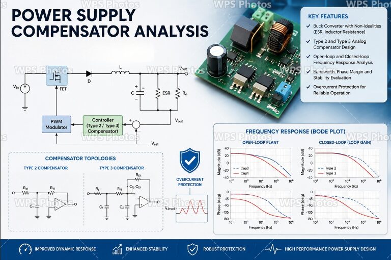
Figure A: Overview of the Proposed Buck Converter Compensation Analysis Framework
Figure A presents the overall conceptual framework of the proposed buck converter compensation analysis developed using the PLECS simulation environment. The illustration integrates the voltage-mode buck converter topology, PWM modulation scheme, Type-II and Type-III analog compensator architectures, overcurrent protection mechanism, and representative frequency-response characteristics. It highlights the interaction between the power stage and the feedback controller while emphasizing the evaluation of crossover frequency, phase margin, gain slope, and system bandwidth through Bode plot analysis. The figure also summarizes the comparative investigation of both compensator designs under different output capacitor and ESR conditions, providing an overview of the methodology adopted to assess converter stability, transient performance, and overall control effectiveness in modern switching power supply applications.
Among various converter topologies, the buck converter is recognized as one of the simplest and most efficient switching converters for stepping down DC voltage. Its widespread adoption results from its straightforward implementation, reduced component count, high efficiency, and compatibility with numerous digital and analog control techniques [2]. Nevertheless, the dynamic characteristics of a buck converter are highly dependent upon the interaction between the inductor, output capacitor, switching frequency, load resistance, and parasitic elements such as the equivalent series resistance (ESR) of the output capacitor. These characteristics introduce poles and zeros into the system transfer function that significantly affect closed-loop stability and transient performance [3].
As converter switching frequencies continue to increase in pursuit of higher power density and smaller passive components, controller design becomes considerably more challenging. Improper controller selection may lead to oscillatory behavior, excessive overshoot, slow transient response, insufficient phase margin, or complete instability. Therefore, systematic compensator design has become a critical aspect of modern switched-mode power supply development [4].
Analog compensation techniques continue to be widely adopted in commercial voltage regulators because of their low implementation cost, high reliability, continuous-time operation, and relatively simple hardware realization. Among the available compensation techniques, Type-II and Type-III compensators are considered the most practical solutions for voltage-mode controlled buck converters [5]. Although both compensators aim to improve stability and transient response, they differ significantly in their pole-zero configurations, achievable phase boost, crossover frequency capability, and suitability for different converter operating conditions.
The Type-II compensator is generally appropriate for converters in which the crossover frequency is higher than the ESR zero frequency. By introducing one compensating zero and two poles, including one pole at the origin, the controller effectively improves steady-state regulation while providing moderate phase compensation. This configuration performs satisfactorily for systems whose plant characteristics do not require excessive phase boost [6].
In contrast, the Type-III compensator incorporates two zeros and three poles, allowing substantially greater phase enhancement around the crossover frequency. This additional flexibility enables designers to compensate converters exhibiting more complex frequency responses, particularly when the crossover frequency falls below the ESR zero. Consequently, Type-III compensation has become the preferred approach for high-bandwidth voltage regulators operating at elevated switching frequencies [7].
The design of power supply compensators is generally based on frequency-domain analysis using Bode plots. Parameters including crossover frequency, gain slope, bandwidth, and phase margin provide valuable information regarding system robustness and dynamic behavior. A properly designed control system typically exhibits a crossover frequency between one-tenth and one-fifth of the switching frequency, a gain slope approaching –20 dB/decade near crossover, and a phase margin exceeding 45°, thereby ensuring satisfactory transient response and adequate stability [8].
Simulation platforms have become essential tools for validating controller performance before hardware implementation. Among available simulation environments, PLECS offers specialized libraries for power electronic systems, allowing accurate modeling of switching converters, passive component non-idealities, control systems, modulation strategies, and frequency-response analysis. The availability of integrated Bode analysis, impulse response evaluation, and multitone excitation makes PLECS particularly suitable for compensator design and verification [9].
This research investigates the performance of Type-II and Type-III analog compensators implemented in a voltage-mode buck converter developed in PLECS. Two converter configurations with different output capacitor values and ESR characteristics are analyzed to evaluate the influence of passive component selection on overall system stability. Both open-loop and closed-loop analyses are conducted to determine the effects of controller selection on crossover frequency, gain slope, phase margin, and bandwidth.
Unlike many previous studies that emphasize mathematical derivations, this work focuses on practical controller evaluation using realistic converter models incorporating passive component non-idealities and protection mechanisms. The comparative study provides engineers with practical design insights that can simplify controller selection for industrial switching power supplies.
The primary objectives of this research are summarized as follows:
- To investigate the frequency response characteristics of a voltage-mode buck converter considering output capacitor ESR.
- To compare the performance of Type-II and Type-III analog compensators under different operating conditions.
- To analyze the influence of capacitor selection on crossover frequency and stability margins.
- To evaluate open-loop and closed-loop converter responses using PLECS frequency-response analysis.
- To demonstrate the effectiveness of proper pole-zero placement in achieving stable converter operation.
- To assess the contribution of overcurrent protection toward converter reliability.
The outcomes of this investigation provide practical guidance for controller selection during the design of high-performance switched-mode power supplies while demonstrating the usefulness of simulation-based frequency-domain analysis in modern power electronics research.
II. Literature Review
Control system design for switching power converters has attracted extensive attention over the past several decades because converter stability directly influences efficiency, reliability, electromagnetic compatibility, and transient performance. Researchers have proposed numerous analog and digital compensation techniques to improve converter dynamics while maintaining robust voltage regulation under varying operating conditions.
Early investigations into switched-mode power supplies primarily focused on small-signal modeling techniques that simplified nonlinear switching behavior into linear frequency-domain representations suitable for controller design [10]. These models enabled designers to identify dominant poles and zeros associated with passive energy storage elements and formed the theoretical foundation for modern compensator development.
Erickson and Maksimović [11] presented comprehensive analytical methods for modeling PWM converters and demonstrated the importance of frequency-response analysis in designing stable closed-loop controllers. Their work established the relationship between converter parameters and dynamic performance, becoming one of the most influential references in power electronics.
Subsequent research introduced practical analog compensator design procedures specifically tailored for voltage-mode buck converters. Rahimi et al. [12] proposed systematic methods for designing Type-II and Type-III compensators by strategically positioning controller poles and zeros according to converter resonant frequencies and ESR characteristics. Their design methodology significantly simplified practical controller implementation and has been widely adopted in industrial voltage regulator applications.
Studies comparing various compensation techniques indicate that Type-II compensators provide adequate performance for converters exhibiting relatively simple frequency characteristics, whereas Type-III compensators offer considerably greater phase boost and improved bandwidth for more demanding applications [13]. These findings have been confirmed through both simulation and experimental validation.
Recent developments have increasingly focused on digital control techniques implemented using digital signal processors and field-programmable gate arrays. Although digital controllers offer flexibility and adaptive capabilities, analog compensators remain widely used because of their low cost, continuous-time operation, reduced computational requirements, and straightforward implementation [14].
Simulation-based controller verification has also become increasingly important in industrial converter design. Modern simulation platforms allow designers to evaluate frequency response, transient behavior, component tolerances, and protection mechanisms before prototype construction, thereby reducing development time and cost [15].
Despite substantial advances in converter control, compensator selection remains highly dependent on converter parameters, switching frequency, passive component characteristics, and desired bandwidth. Consequently, comparative studies examining the practical performance of Type-II and Type-III compensators continue to provide valuable design guidance for engineers developing high-performance switching power supplies.
The following section presents the operating principles of the investigated buck converter together with the mathematical modeling and compensator design methodology adopted in this research.
III. Buck Converter Modeling and Control Architecture
A. Operating Principle of the Buck Converter
The buck converter is one of the most widely implemented non-isolated DC-DC converter topologies due to its high conversion efficiency, compact structure, and excellent voltage regulation capability. It converts a higher input DC voltage into a lower regulated output voltage through high-frequency switching of a semiconductor device. Because of its simplicity and high efficiency, the buck converter has become the preferred choice for distributed power systems, communication equipment, industrial automation, battery-powered electronics, renewable energy systems, automotive electronics, and embedded control applications [1], [2].
The converter investigated in this work consists of a controlled MOSFET switch, freewheeling diode, inductor, output capacitor, resistive load, PWM modulator, voltage feedback network, and analog compensation circuit. Unlike ideal converter models, the simulated system also incorporates practical component non-idealities including the inductor winding resistance and the equivalent series resistance (ESR) of the output capacitor. These parasitic parameters significantly influence the frequency response of the converter and therefore must be considered during controller design [3].
During the ON interval of the switching cycle, the MOSFET conducts and connects the input source directly to the inductor. The inductor stores magnetic energy while simultaneously supplying current to both the output capacitor and the load. During the OFF interval, the MOSFET is turned off and the inductor releases its stored energy through the freewheeling diode, maintaining continuous current flow to the load. The output capacitor smooths the voltage ripple by absorbing and supplying current according to instantaneous load demand.
The duty ratio generated by the PWM modulator determines the average output voltage. However, disturbances caused by input voltage variations, load transients, and component tolerances continuously affect converter operation. Consequently, a feedback controller is necessary to regulate the duty cycle and maintain the desired output voltage under varying operating conditions [4].
B. Small-Signal Modeling
Although switching converters operate as nonlinear systems because of periodic switching, controller design is typically performed using small-signal linearization around a steady-state operating point. This approach converts the nonlinear converter into an equivalent linear dynamic model that accurately represents its behavior within the frequency range of interest [5].
Small-signal modeling enables designers to investigate converter stability using classical control techniques such as Bode plots, Nyquist diagrams, and root-locus analysis. The resulting transfer function describes how variations in duty cycle influence the output voltage while accounting for passive energy storage components and parasitic resistances.
For the investigated buck converter, the output filter introduces two dominant poles that originate from the inductor-capacitor network. In addition, the ESR of the output capacitor generates an additional zero that substantially modifies the phase response of the plant. Depending on its location relative to the desired crossover frequency, this ESR zero may either improve or degrade closed-loop stability [6].
The converter analyzed in this research therefore represents a practical rather than an idealized system, making the obtained simulation results more representative of real switching power supplies.
C. Plant Transfer Function
The dynamic relationship between the converter duty cycle and output voltage is represented by the small-signal control-to-output transfer function. This mathematical model forms the foundation for compensator design because it identifies the dominant poles and zero that determine converter stability.
The simplified plant transfer function of the voltage-mode buck converter is expressed as

Where:
- G_plant(s) = Small-signal control-to-output transfer function
- s = Laplace operator (complex frequency variable)
- L = Output filter inductance (H)
- C_total = Total output capacitance (F)
- R_o = Load resistance (Ω)
- ESR = Equivalent Series Resistance of the output capacitor (Ω)
Equation (1) illustrates that converter dynamics are governed by the interaction between the output filter and capacitor parasitic resistance. The quadratic denominator represents the second-order LC dynamics, while the numerator introduces an ESR-generated zero that modifies the converter phase response. This transfer function serves as the basis for designing both Type-II and Type-III compensators by enabling accurate pole-zero placement for improved stability [12].
D. Influence of Output Capacitor ESR
The equivalent series resistance of the output capacitor is often regarded as an undesirable parasitic element because it increases output voltage ripple and power loss. Nevertheless, from a control perspective, ESR introduces a left-half-plane zero that may provide beneficial phase lead depending on its frequency location.
If the ESR zero occurs above the desired crossover frequency, its influence on system dynamics is relatively small. Conversely, when the ESR zero approaches the crossover frequency, the additional phase contribution can substantially affect controller design. Improper consideration of this effect may reduce stability margins or even result in oscillatory converter behavior [7].
The PLECS model evaluates two different capacitor configurations to investigate these effects. The first system employs a larger output capacitance with relatively higher stored energy, whereas the second utilizes a smaller capacitor possessing different ESR characteristics. These configurations provide distinct frequency responses that demonstrate the necessity of selecting an appropriate compensator according to converter parameters.
IV. Design of Analog Compensators
A. Importance of Compensation
The uncompensated buck converter generally exhibits insufficient phase margin and limited bandwidth for high-performance voltage regulation. Without compensation, the converter may experience excessive overshoot, oscillatory response, prolonged settling time, or instability during sudden load variations [8].
A compensator modifies the open-loop frequency response by introducing additional poles and zeros that reshape the gain and phase characteristics of the system. Proper compensation ensures adequate stability while simultaneously improving transient response and disturbance rejection.
The principal design objectives adopted in this research include:
- Achieving a crossover frequency between one-tenth and one-fifth of the switching frequency.
- Maintaining a gain slope close to −20 dB/decade near crossover.
- Obtaining a phase margin greater than 45°.
- Improving transient response without sacrificing stability.
- Ensuring robust operation under practical component tolerances.
These criteria represent commonly accepted guidelines for voltage-mode switching power supplies [9].
B. Type-II Analog Compensator
The Type-II compensator is one of the simplest analog compensation techniques used in voltage-mode power converters. It consists of one compensating zero and two poles, including one pole located at the origin. This configuration increases low-frequency gain while providing sufficient phase lead for converters exhibiting relatively simple dynamic characteristics.
Within the investigated PLECS model, the Type-II compensator employs an operational amplifier together with resistive and capacitive feedback elements. The output voltage is sensed through a resistive divider and compared with a fixed reference voltage. The resulting error signal is processed by the compensator before being supplied to the PWM modulator.
The compensating zero is positioned close to the resonant frequency of the LC filter to cancel one of the dominant plant poles. Meanwhile, the high-frequency pole suppresses switching noise and minimizes amplification of high-frequency disturbances. Proper placement of these frequency-shaping elements significantly improves converter stability while maintaining accurate voltage regulation.
The Type-II compensator performs particularly well when the desired crossover frequency is located above the ESR zero frequency. Under these operating conditions, the converter naturally benefits from the phase contribution of the ESR zero, requiring only moderate additional compensation [12].
C. Type-III Analog Compensator
As converter bandwidth requirements continue to increase, Type-II compensation often becomes insufficient because it cannot generate enough phase boost near the crossover frequency. This limitation becomes especially significant when the crossover frequency lies below the ESR zero.
To overcome this problem, the Type-III compensator introduces an additional zero and an additional high-frequency pole, providing considerably greater flexibility in shaping the converter frequency response.
The generalized transfer function of the Type-III compensator is represented by

Where:
- H_Type3(s) = Type-III compensator transfer function
- s = Laplace operator
- ω_z1 = Angular frequency of the first compensating zero (rad/s)
- ω_z2 = Angular frequency of the second compensating zero (rad/s)
- ω_p2 = Angular frequency of the second pole (rad/s)
- ω_p3 = Angular frequency of the third pole (rad/s)
Equation (2) shows that the additional pole-zero pair enables substantially greater phase compensation compared with the Type-II controller. By carefully positioning these frequencies relative to the LC resonant frequency and the ESR zero, the designer can obtain larger bandwidth while preserving satisfactory stability margins [12].
D. Comparison Between Type-II and Type-III Controllers
Although both compensators seek to stabilize the buck converter, their operating characteristics differ considerably.
The Type-II controller provides a relatively simple implementation with fewer passive components and straightforward tuning. It is generally preferred for converters having moderate bandwidth requirements and plant responses that already possess adequate phase margin.
The Type-III controller offers significantly greater design flexibility by introducing an additional pole-zero pair. This configuration enables higher crossover frequencies, larger phase margins, improved transient response, and superior robustness under varying operating conditions. However, the increased number of passive components also makes parameter selection more critical.
For converters employing small output capacitors or operating at high switching frequencies, the Type-III compensator generally achieves superior dynamic performance because it can compensate for the phase lag introduced by the LC filter more effectively than the Type-II controller [13], [14].
V. PLECS-Based Control Architecture
The complete simulation model is implemented using the PLECS simulation platform, which combines electrical circuit modeling with control system design in a unified environment. The converter model consists of the power stage, PWM modulator, voltage sensing network, analog compensator, and protection circuitry.
A manual switching block allows the simulation to alternate between open-loop and closed-loop operation, facilitating both plant characterization and controller verification. During open-loop analysis, frequency-response techniques such as multitone excitation and impulse response analysis generate the converter Bode plot directly from the simulation model. These analyses enable accurate determination of crossover frequency, gain slope, resonant behavior, and phase margin without requiring hardware implementation.
For closed-loop evaluation, either the Type-II or Type-III compensator is connected to the voltage feedback loop. This arrangement permits direct comparison of both controller structures under identical operating conditions, ensuring a consistent and reliable assessment of their dynamic performance.
The subsequent section presents comprehensive simulation results obtained from both open-loop and closed-loop analyses, followed by a detailed discussion of converter stability, frequency response, and compensator effectiveness.
You can download the Project files here: Download files now. (You must be logged in).
VI. Simulation Methodology
The proposed buck converter and compensation circuits were modeled and analyzed using the PLECS simulation environment. PLECS provides an integrated platform for power electronic circuit modeling, controller implementation, and frequency-domain analysis, making it particularly suitable for evaluating switching power supplies. The simulation model includes the complete power stage, PWM modulator, analog compensation network, voltage feedback loop, and overcurrent protection circuit. Practical non-idealities such as the output capacitor equivalent series resistance (ESR) and inductor resistance were incorporated to emulate realistic converter behavior.
The objective of the simulation study is to compare the dynamic performance of Type-II and Type-III analog compensators under different output filter conditions. Two capacitor configurations are investigated in order to evaluate the influence of output capacitance and ESR on the converter frequency response. The larger capacitor configuration represents a converter with lower resonant frequency and higher stored energy, while the smaller capacitor configuration exhibits a higher resonant frequency and different ESR characteristics.
The simulation procedure consists of two major stages. The first stage investigates the uncompensated converter using open-loop frequency-response analysis. During this stage, the plant transfer function is obtained directly from the converter model through multitone excitation and impulse response analysis. The generated Bode plots are used to determine the crossover frequency, gain slope, resonant characteristics, and phase margin before compensation.
The second stage evaluates the complete closed-loop converter by introducing either the Type-II or Type-III compensator into the feedback loop. The frequency response is again obtained through loop gain analysis, allowing direct comparison of both controller structures under identical operating conditions. Since all simulations employ the same converter hardware and operating parameters, any observed performance differences are attributed solely to the compensation strategy.
The converter is also equipped with an overcurrent protection circuit that continuously monitors the inductor current. Whenever the current exceeds the specified protection threshold, the PWM modulation signal is immediately disabled, forcing the converter to stop switching temporarily. After a predefined delay, normal switching operation automatically resumes. This protection mechanism enhances converter reliability by preventing excessive current stress during overload or fault conditions.
The simulation methodology adopted in this study follows practical controller design procedures commonly used in industrial switched-mode power supply development. Rather than relying exclusively on mathematical derivations, the controller performance is verified using frequency-domain simulation, enabling direct observation of gain margin, phase margin, bandwidth, and crossover frequency.
VII. Results and Discussion
A. Open-Loop Frequency Response Analysis
The first stage of the investigation focuses on the uncompensated buck converter. Frequency-response analysis is performed using the control-to-output transfer function of the converter to evaluate its inherent dynamic characteristics before introducing feedback compensation.
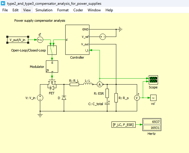
Figure 1: Open Loop Type II Power Supply Compensator analysis in PLECS
Figure 1 presents the open-loop analysis model of the Type-II power supply compensator developed in the PLECS simulation environment. The model includes the buck converter power stage and the control path used to evaluate the plant frequency response, providing the basis for compensator design and stability assessment before closing the feedback loop.
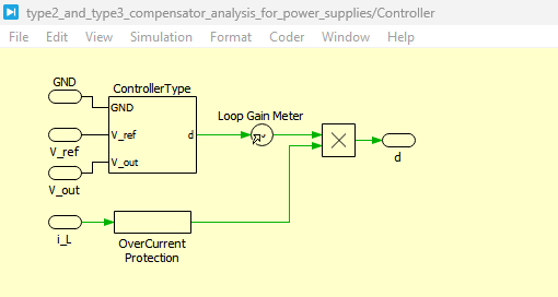
Figure 2: Open Loop Type II Power Supply Compensator Controller design in PLECS simulation
Figure 2 presents the Type-II analog compensator controller implemented in PLECS using an operational amplifier with resistor-capacitor (RC) compensation networks. The controller is designed to improve converter stability by introducing appropriate poles and zeros, thereby enhancing phase margin and dynamic response.
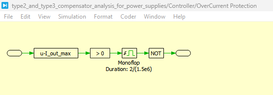
Figure 3: Open Loop Type II Power Supply Compensator Controller with over current Protection circuit
Figure 3 presents the complete open-loop Type-II compensator integrated with an overcurrent protection circuit in the PLECS model. The protection mechanism continuously monitors the inductor current and disables the switching signal whenever the current exceeds the predefined safety limit, ensuring reliable converter operation under overload conditions.
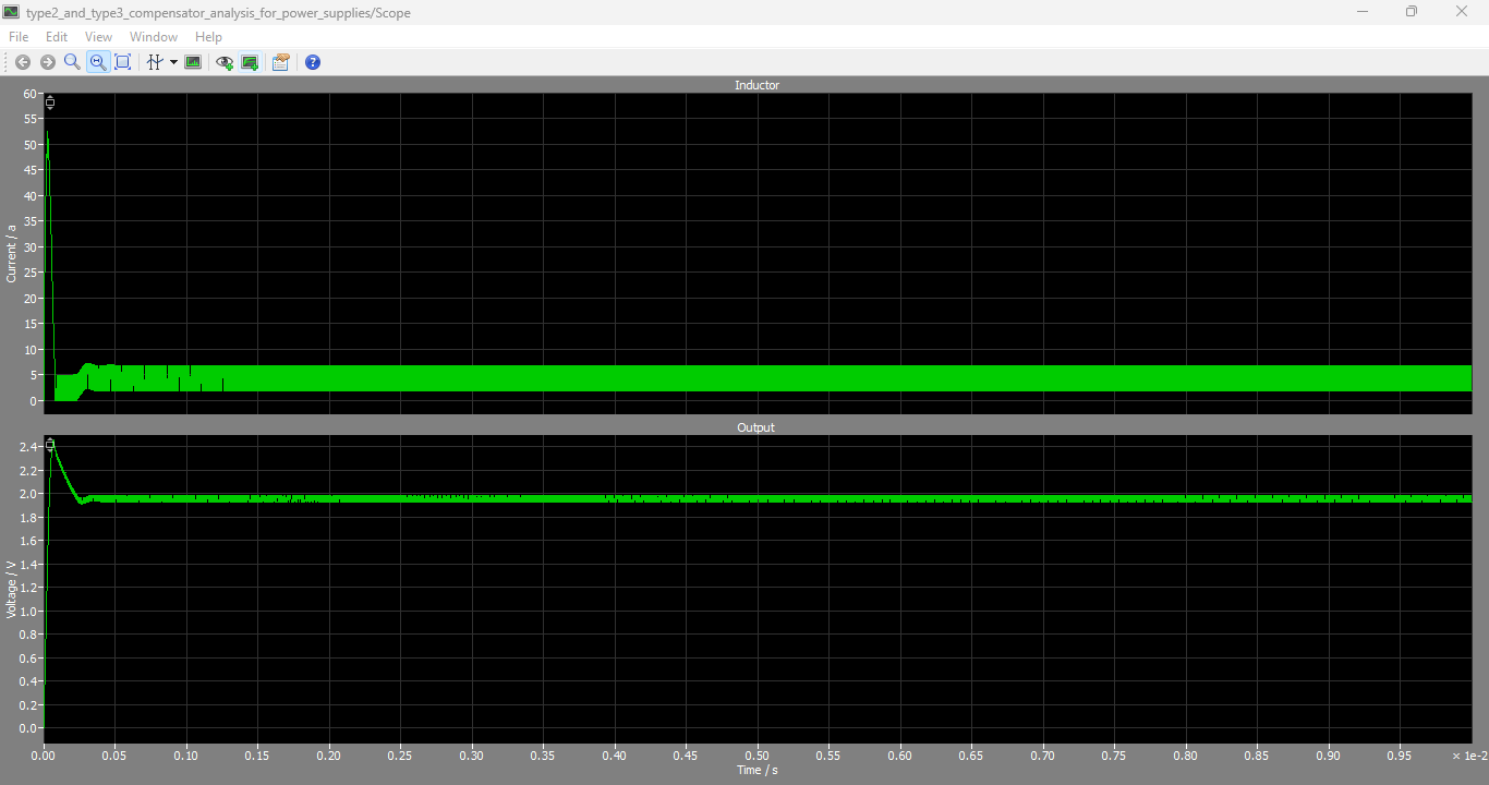
Figure 4: Open loop Type II Power Supply Compensator Output Current and Voltage graphs
Figure 4 presents the simulated output voltage and inductor current waveforms of the open-loop Type-II compensated buck converter. The graphs illustrate the converter’s electrical response under open-loop operation and provide insight into the voltage regulation and current characteristics before closed-loop feedback is applied.
For the first capacitor configuration, the Bode plot indicates that the crossover frequency is approximately 40 kHz. The gain decreases at nearly −20 dB per decade around the crossover frequency, while the corresponding phase margin approaches 95°. Such a large phase margin indicates excellent stability; however, the relatively low crossover frequency limits the dynamic response of the converter. Since the crossover frequency remains significantly below one-tenth of the switching frequency, the transient response is slower than desired for high-performance voltage regulation.
When the output capacitor is changed to the second configuration, the frequency response changes considerably. The crossover frequency increases to approximately 60 kHz, indicating a wider system bandwidth and improved transient response. Nevertheless, the gain slope around the crossover frequency becomes nearly −40 dB per decade. Although the phase margin remains close to 50°, the steeper gain slope indicates increased sensitivity to parameter variations and potential degradation of closed-loop robustness.
These observations demonstrate that passive component selection alone can significantly alter converter dynamics. Consequently, a properly designed compensator becomes essential for maintaining adequate stability while achieving the desired transient performance.
You can download the Project files here: Download files now. (You must be logged in).
B. Closed-Loop Analysis of System 1
After completing the open-loop evaluation, the converter is configured for closed-loop operation using the first output capacitor configuration. Initially, the Type-II compensator is connected within the voltage feedback loop.
The resulting loop gain analysis indicates that the crossover frequency increases to approximately 65 kHz. The gain slope near the crossover frequency approaches the desired value of −20 dB per decade, while the phase margin improves to nearly 65°. These characteristics satisfy the commonly accepted design criteria for voltage-mode power converters, indicating that the controller successfully stabilizes the converter while simultaneously improving dynamic response.
The increased bandwidth enables the converter to respond more rapidly to load disturbances and reference voltage changes without introducing excessive overshoot or oscillations. The improved phase margin further ensures stable operation over a broad operating range despite practical component tolerances.
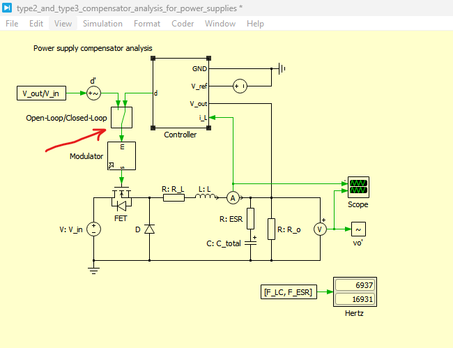
Figure 5: Closed Loop Type III Power Supply Compensator analysis in PLECS
Figure 5 presents the closed-loop configuration of the Type-III power supply compensator implemented in PLECS. The model demonstrates the integration of the feedback controller with the buck converter, enabling detailed analysis of system stability, crossover frequency, bandwidth, and phase margin under closed-loop operation.
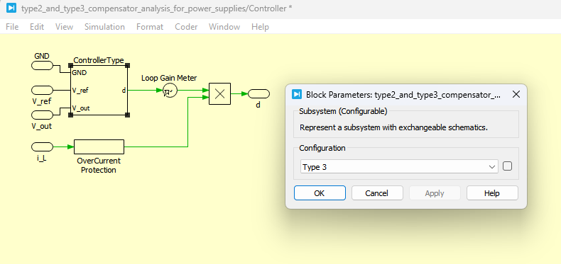
Figure 6: Closed Loop Type III Power Supply Compensator Controller design in PLECS simulation
Figure 6 presents the Type-III compensator controller designed using an operational amplifier and multiple RC networks in the PLECS environment. The additional pole-zero pair provides enhanced phase compensation, allowing the converter to achieve improved transient response and stable operation at higher crossover frequencies.
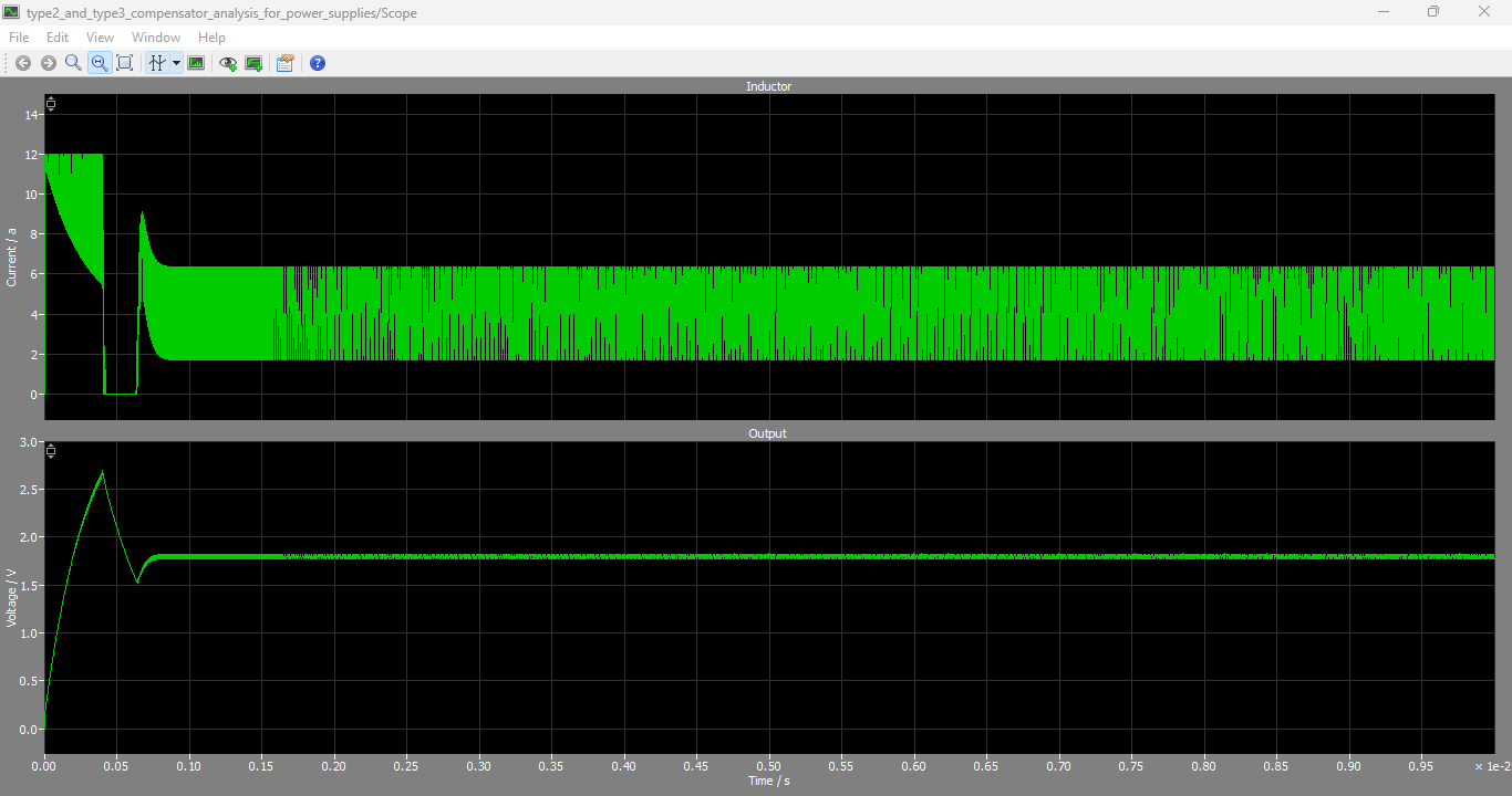
Figure 7: Closed loop Type III Power Supply Compensator Output Current and Voltage graphs
You can download the Project files here: Download files now. (You must be logged in).
Figure 7 presents the simulated output voltage and inductor current waveforms obtained from the closed-loop Type-III compensated buck converter. The results demonstrate stable voltage regulation, smooth current behavior, and improved dynamic performance, confirming the effectiveness of the Type-III compensator in maintaining reliable converter operation under closed-loop control.
The controller is then replaced by the Type-III compensator while maintaining identical converter parameters. Simulation results show that the crossover frequency further increases to approximately 100 kHz while preserving a gain slope close to −20 dB per decade. The phase margin remains near 65°, demonstrating that the additional pole-zero pair introduced by the Type-III compensator allows substantially greater bandwidth without sacrificing stability.
Although both compensators satisfy the design objectives for System 1, the Type-III controller exhibits faster dynamic response because of its larger crossover frequency. Nevertheless, the Type-II controller remains an attractive solution due to its simpler circuit implementation and lower component count.
C. Closed-Loop Analysis of System 2
The second simulation scenario evaluates the converter using the smaller output capacitor configuration. This configuration modifies the LC resonant frequency and shifts the ESR zero relative to the desired crossover frequency, thereby increasing the complexity of controller design.
The Type-III compensator is first employed because its additional phase boost is expected to improve stability under these conditions. The resulting loop gain analysis indicates a crossover frequency of approximately 75 kHz together with a gain slope close to −20 dB per decade. Furthermore, the measured phase margin remains around 61°, demonstrating satisfactory stability and dynamic performance.
The frequency response confirms that the additional zero provided by the Type-III compensator effectively compensates the phase lag introduced by the LC filter. Consequently, the converter achieves both wide bandwidth and sufficient stability despite the more demanding plant characteristics.
Next, the Type-II compensator is applied to the same converter configuration. Although the crossover frequency increases further to approximately 92 kHz, the corresponding gain slope becomes nearly −40 dB per decade. At the same time, the phase margin decreases dramatically to approximately 25°, indicating that the converter operates very close to instability.
Such a small phase margin would likely produce excessive overshoot, oscillatory transient response, increased sensitivity to component tolerances, and poor disturbance rejection in practical hardware. These observations clearly demonstrate that the Type-II compensator cannot provide sufficient phase boost when the crossover frequency is located below the ESR zero frequency.
D. Comparative Evaluation of Type-II and Type-III Compensators
The simulation results clearly illustrate the differences between the two analog compensation techniques.
The Type-II compensator performs exceptionally well when the converter already possesses favorable frequency characteristics. Its relatively simple pole-zero structure effectively increases low-frequency gain while maintaining acceptable stability margins for converters whose crossover frequency exceeds the ESR zero. Because it requires fewer passive components, implementation complexity and design effort remain comparatively low.
However, the available phase boost provided by the Type-II controller is inherently limited. As converter switching frequencies continue to increase and higher bandwidth becomes desirable, the controller eventually reaches its compensation capability. This limitation becomes particularly evident in System 2, where the controller is unable to maintain adequate phase margin despite achieving a high crossover frequency.
Conversely, the Type-III compensator demonstrates consistently superior performance across both converter configurations. The additional pole-zero pair provides substantially greater flexibility for shaping the loop gain characteristics, allowing simultaneous achievement of high bandwidth and sufficient phase margin.
From a practical engineering perspective, the Type-III controller is therefore better suited for modern high-frequency voltage regulators requiring fast transient response and robust stability under varying operating conditions. Although its implementation requires additional passive components and slightly more complex tuning, the resulting improvement in converter performance generally outweighs the increased design complexity.
E. Effect of Output Capacitor Characteristics
The simulation also emphasizes the significant influence of output capacitor characteristics on converter dynamics. Changing the capacitance and ESR modifies both the resonant frequency and the location of the ESR zero, thereby altering the frequency response of the converter.
Larger capacitance values generally improve output voltage ripple performance but reduce system bandwidth because of lower resonant frequency. Smaller capacitance values increase bandwidth but simultaneously demand more sophisticated compensation techniques to preserve stability.
Similarly, the ESR of the output capacitor contributes an additional zero that may either assist or complicate controller design depending on its relative position with respect to the desired crossover frequency. Designers must therefore consider capacitor parasitic characteristics together with compensator design rather than treating them independently.
F. Performance of the Overcurrent Protection Circuit
Besides voltage regulation, converter reliability is also improved through implementation of the overcurrent protection circuit. The protection logic continuously monitors the inductor current and compares it with a predefined maximum allowable value.
Whenever the current exceeds the specified threshold, the PWM modulation signal is immediately disabled, preventing further energy transfer from the input source to the output stage. After several switching cycles, normal converter operation is automatically restored once the fault condition disappears.
Simulation results indicate that this protection strategy effectively limits excessive current stress without introducing permanent interruption of converter operation. Consequently, semiconductor devices, passive components, and power interconnections remain protected against overload conditions, thereby improving overall converter reliability and operational safety.
VIII. Conclusion
This research presented a comprehensive comparative investigation of Type-II and Type-III analog compensators for voltage-mode controlled buck converters using the PLECS simulation environment. The study examined both uncompensated and compensated converter responses while considering practical component non-idealities including output capacitor equivalent series resistance and inductor resistance.
Open-loop analysis demonstrated that passive component selection substantially influences converter frequency response, crossover frequency, gain slope, and phase margin. Although both investigated capacitor configurations produced stable open-loop characteristics, neither achieved the desired combination of bandwidth and dynamic response without compensation.
Closed-loop simulation results confirmed that the Type-II compensator provides excellent performance when the converter crossover frequency is located above the ESR zero. Under these conditions, the controller successfully achieved the desired gain slope, acceptable bandwidth, and sufficient phase margin while maintaining relatively simple circuit implementation.
However, when converter dynamics became more demanding because of different output capacitor characteristics, the Type-II compensator failed to provide adequate phase compensation. The reduced phase margin and steeper gain slope indicated that the converter approached instability despite the increased crossover frequency.
In contrast, the Type-III compensator consistently demonstrated superior dynamic performance under both operating conditions. The additional pole-zero pair provided greater design flexibility, enabling higher bandwidth together with satisfactory stability margins. Consequently, the Type-III controller proved particularly suitable for high-frequency switching converters requiring rapid transient response and robust operation.
The inclusion of overcurrent protection further enhanced converter reliability by preventing excessive current stress during abnormal operating conditions. Overall, the simulation results demonstrate that successful compensator design requires careful consideration of both converter dynamics and passive component characteristics.
The presented investigation provides practical guidance for selecting appropriate analog compensators during the design of modern switched-mode power supplies. Future work may extend this study by implementing the controllers on experimental hardware, investigating digital compensation techniques, and evaluating adaptive control strategies for variable operating conditions.
References
[1] A. M. Rahimi, P. Parto, and P. Asadi, Compensator Design Procedure for Buck Converter with Voltage-Mode Error Amplifier, International Rectifier Application Note AN-1162.
[2] R. W. Erickson and D. Maksimović, Fundamentals of Power Electronics, 2nd ed. New York, NY, USA: Springer, 2001.
[3] N. Mohan, T. M. Undeland, and W. P. Robbins, Power Electronics: Converters, Applications and Design, 3rd ed. Hoboken, NJ, USA: Wiley, 2003.
[4] D. M. Mitchell, DC-DC Switching Regulator Analysis. New York, NY, USA: McGraw-Hill, 1998.
[5] C. K. Tse, Complex Behavior of Switching Power Converters. Boca Raton, FL, USA: CRC Press, 2003.
[6] R. Redl and N. O. Sokal, “Near-optimum dynamic regulation of DC-DC converters using feed-forward of output current,” IEEE Transactions on Power Electronics, vol. 1, no. 3, pp. 181–192, 1986.
[7] R. Ridley, “A new continuous-time model for current-mode control,” IEEE Transactions on Power Electronics, vol. 6, no. 2, pp. 271–280, 1991.
[8] F. C. Lee, “High-frequency quasi-resonant converter technologies,” Proceedings of the IEEE, vol. 76, no. 4, pp. 377–390, 1988.
[9] R. D. Middlebrook and S. Ćuk, “A general unified approach to modelling switching-converter power stages,” in Proc. IEEE Power Electronics Specialists Conference, 1976, pp. 18–34.
[10] V. Vorpérian, Fast Analytical Techniques for Electrical and Electronic Circuits. Cambridge, U.K.: Cambridge Univ. Press, 2002.
[11] B. Bryant and M. K. Kazimierczuk, “Voltage-loop power-stage transfer functions with MOSFET delay for PWM DC-DC converters,” IEEE Transactions on Industrial Electronics, vol. 54, no. 1, pp. 347–353, 2007.
[12] PLECS User Documentation, Plexim GmbH, Zurich, Switzerland, 2023.
[13] R. B. Ridley, Loop Control for Switching Power Supplies. Ridley Engineering Inc., 2014.
[14] M. K. Kazimierczuk, Pulse-Width Modulated DC–DC Power Converters. Hoboken, NJ, USA: Wiley, 2015.
[15] S. Buso and P. Mattavelli, Digital Control in Power Electronics, 2nd ed. San Rafael, CA, USA: Morgan & Claypool, 2015.
You can download the Project files here: Download files now. (You must be logged in).







Responses