

Digital Control and Thermal Performance Analysis of a Grid-Connected Single-Phase Battery Charger Using Cascaded AC/DC and Phase-Shifted DC/DC Converters in PLECS

Author: Waqas Javaid
Abstract
The rapid growth of electric vehicles, renewable energy systems, and battery energy storage technologies has significantly increased the demand for efficient and reliable battery charging systems. Modern battery chargers are expected to achieve high conversion efficiency, near-unity power factor, excellent output voltage regulation, and high reliability while maintaining compact size and low thermal stress. This paper presents the modeling and simulation of a grid-connected single-phase battery charger developed in the PLECS simulation environment. The proposed charger consists of a cascaded architecture including an interleaved boost AC/DC power factor correction (PFC) converter followed by a phase-shifted resonant DC/DC converter. The front-end converter regulates the DC-link voltage at 300 V while maintaining sinusoidal input current synchronized with the utility voltage. The isolated DC/DC converter delivers a regulated output voltage up to 120 V with a rated output power of approximately 1.4 kW suitable for battery charging applications.
A cascaded digital control strategy employing proportional-integral (PI) controllers is implemented to regulate both voltage and current loops. Furthermore, thermal models of semiconductor devices including MOSFETs and output diodes are incorporated to investigate junction temperature and heat dissipation characteristics during operation. Simulation studies are carried out under varying operating conditions including output voltage reference changes and load disturbances. The obtained results demonstrate stable DC-link voltage regulation, rapid transient response, high power factor, accurate output voltage tracking, and effective thermal performance. The developed PLECS model provides an efficient platform for evaluating converter performance, digital control algorithms, and thermal characteristics prior to hardware implementation.
I. Introduction
The increasing penetration of electric vehicles (EVs), renewable energy generation systems, smart grids, and battery energy storage systems has accelerated the development of advanced battery charging technologies. Battery chargers serve as the interface between the electrical grid and rechargeable batteries, directly influencing charging efficiency, battery lifetime, system reliability, and overall energy utilization. Modern charging systems must satisfy stringent performance requirements, including high conversion efficiency, low harmonic distortion, fast dynamic response, and compliance with international power quality standards such as IEC 61000-3-2 and IEEE recommendations [1]–[3].
Conventional battery chargers often suffer from poor power factor, increased harmonic distortion, excessive switching losses, and inadequate thermal management, especially under high-power operating conditions. As charging power increases for electric mobility and industrial energy storage applications, efficient converter topologies and advanced control strategies become essential. Cascaded power conversion architectures have therefore become one of the preferred solutions because they separate the objectives of input power quality improvement and output voltage regulation while allowing independent optimization of each converter stage [4].
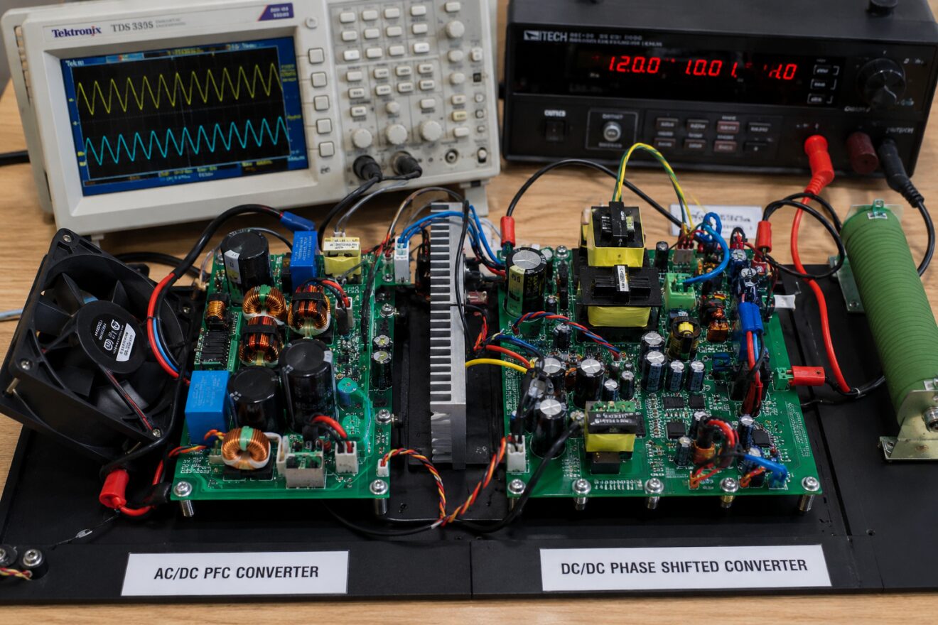
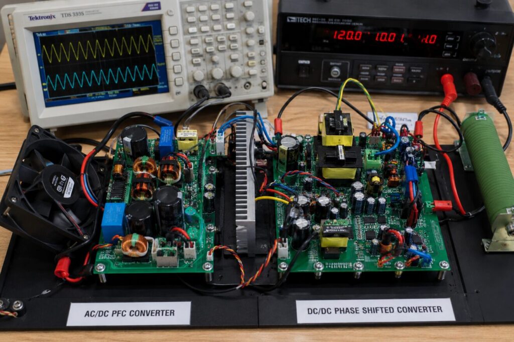
Figure 1: Experimental Prototype of the Proposed Single-Phase Grid-Connected Battery Charger
Figure 1 presents the experimental hardware prototype of the proposed single-phase battery charger, comprising an interleaved AC/DC power factor correction (PFC) converter and an isolated phase-shifted DC/DC converter. The setup includes the power converter boards, magnetic components, cooling system, programmable DC power supply, and digital oscilloscope used to evaluate the converter performance under controlled laboratory conditions. This experimental configuration closely represents a practical battery charging system and serves as the hardware platform for validating the proposed converter architecture and control strategy.
The front-end AC/DC converter is primarily responsible for correcting the input power factor while maintaining a regulated DC-link voltage. Among various power factor correction techniques, the interleaved boost converter has become particularly attractive due to its lower input current ripple, improved current sharing, reduced electromagnetic interference (EMI), and higher efficiency compared with conventional single-channel boost converters [5]. Interleaving distributes the total current among multiple switching phases, thereby reducing current stress on individual semiconductor devices and minimizing passive component size.
The second stage generally consists of an isolated DC/DC converter that provides galvanic isolation, voltage transformation, and precise output voltage regulation required for battery charging. Phase-shifted resonant converters have attracted considerable attention because of their ability to achieve soft switching over a wide operating range. Zero-voltage switching (ZVS) significantly reduces switching losses and electromagnetic interference while enabling high-frequency operation, resulting in increased power density and improved converter efficiency [6], [7]. These characteristics make resonant converters highly suitable for high-power battery charging applications where efficiency and thermal performance are critical design objectives.
Digital control techniques have increasingly replaced conventional analog controllers because of their flexibility, programmability, robustness, and ease of implementation. Digital proportional-integral (PI) controllers offer accurate voltage regulation while simplifying controller parameter tuning and system integration. In cascaded converter systems, multiple feedback loops are employed to independently regulate voltage and current, ensuring stable operation during load transients and reference changes [8]. Anti-windup mechanisms further enhance controller stability by preventing excessive integrator accumulation during saturation conditions.
Thermal management has become another critical aspect of modern power electronic converter design. Semiconductor devices such as MOSFETs and power diodes experience considerable conduction and switching losses during operation. Excessive junction temperatures accelerate device degradation, reduce reliability, and shorten system lifetime. Consequently, accurate thermal modeling enables designers to evaluate junction temperatures, optimize heat sink selection, and predict converter reliability before hardware implementation [9]. Simulation platforms capable of simultaneously analyzing electrical and thermal behavior provide valuable insight into system performance under realistic operating conditions.
Among available simulation platforms, PLECS has become widely adopted for power electronic system development because of its efficient solver architecture, comprehensive component libraries, and integrated thermal modeling capability [10]. Unlike traditional simulation tools, PLECS allows electrical, magnetic, control, and thermal domains to be simulated simultaneously within a unified environment. This significantly simplifies the design process while reducing computational complexity.
This research investigates a grid-connected single-phase battery charger developed using the PLECS simulation environment. The proposed charger consists of two cascaded conversion stages. The first stage is an interleaved boost power factor correction converter responsible for maintaining a constant DC bus voltage of 300 V while ensuring nearly sinusoidal grid current. The second stage is a phase-shifted resonant DC/DC converter that regulates the battery charging voltage up to 120 V at an output power rating of approximately 1.4 kW. Digital PI controllers regulate both conversion stages through cascaded voltage and current control loops to achieve stable operation under varying load conditions.
The main contributions of this work are summarized as follows:
- Development of a complete grid-connected single-phase battery charger using cascaded AC/DC and DC/DC converters in the PLECS environment.
- Implementation of digital cascaded PI controllers for simultaneous power factor correction and output voltage regulation.
- Integration of detailed thermal models for MOSFETs, power diodes, and common heat sink analysis.
- Performance evaluation under output voltage reference changes and varying load conditions.
- Demonstration of stable DC bus regulation, high power factor, accurate output voltage control, and reliable thermal operation suitable for high-power battery charging applications.
II. System Architecture and Operating Principle
A. Overall Battery Charger Configuration
The proposed battery charging system employs a two-stage power conversion architecture designed to provide high conversion efficiency, excellent power quality, and reliable battery charging performance. As illustrated in Fig. 1, the system consists of a front-end AC/DC power factor correction (PFC) converter followed by an isolated DC/DC converter. The AC/DC stage interfaces directly with the single-phase utility grid and converts the alternating input voltage into a regulated DC-link voltage of 300 V. The second conversion stage further regulates this DC voltage to produce an adjustable battery charging voltage with a maximum output of 120 V and a rated power of approximately 1.4 kW.
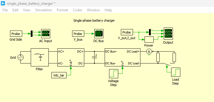
Figure 2: Single phase battery charger circuit developed in PLECS Simulation
Figure 2 illustrates the single-phase battery charger circuit implemented in the PLECS simulation environment. The model consists of a cascaded architecture including an AC/DC power factor correction stage and a DC/DC phase-shifted converter stage. The AC side is connected to the grid through a filter, while the DC side interfaces with the energy storage system. The overall structure enables controlled power flow from the grid to the battery with regulated DC-link voltage and improved power quality.
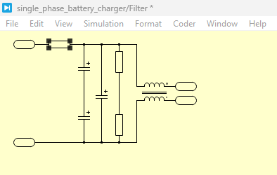
Figure 3: Grid side filter design to remove the noise and provide clean energy to the circuit
Figure 3 presents the grid-side filter design used in the proposed battery charger system. The filter is implemented to suppress high-frequency switching harmonics generated by the power electronic converters. It ensures that only the fundamental component of the grid voltage and current is processed, thereby improving power quality and reducing electromagnetic interference (EMI). The filter also enhances system stability by smoothing the input current waveform.
The cascaded converter configuration enables independent optimization of the grid-side and load-side converters. The AC/DC converter focuses on achieving high input power factor, minimizing harmonic distortion, and regulating the intermediate DC bus voltage. Meanwhile, the DC/DC converter performs electrical isolation, voltage conversion, and precise battery charging regulation. This separation of control objectives significantly improves the dynamic performance of the overall charging system while simplifying controller design.
The overall system also includes digital control units, measurement blocks, feedback networks, gate pulse generation circuits, output filters, and thermal models of semiconductor devices. The digital controllers continuously monitor the DC-link voltage, converter currents, and output voltage to maintain stable operation under varying load conditions. Such an architecture provides flexibility for implementing different charging algorithms while maintaining excellent steady-state and transient performance.
Another significant advantage of the proposed topology is its modularity. Each converter stage can be independently modified or upgraded without affecting the overall system structure. This feature makes the architecture suitable for a wide range of battery charging applications including electric vehicles, renewable energy storage systems, industrial battery chargers, and uninterrupted power supply (UPS) systems.
B. AC/DC Interleaved Power Factor Correction Converter
The first stage of the battery charger consists of an interleaved boost power factor correction converter, as shown in Figure 4. This converter performs three primary functions: conversion of AC input power into regulated DC power, correction of input power factor, and stabilization of the intermediate DC bus voltage.
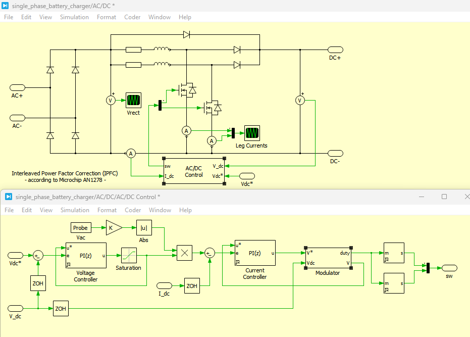
Figure 4: AC to DC convert circuit and DC control circuit developed in PLECS
Figure 4 shows the AC-to-DC conversion stage along with the associated digital control circuit developed in PLECS. The AC/DC converter operates as a power factor correction (PFC) stage that regulates the DC-link voltage. The control circuit processes voltage and current feedback signals and generates appropriate switching signals to maintain sinusoidal input current and stable DC bus voltage.
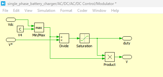
Figure 5: Modulator design of DC control in PLECS
Figure 5 illustrates the modulator design used in the DC control system. The modulator converts the control signals generated by the digital PI controller into PWM switching pulses. These pulses drive the semiconductor switches of the converter. The modulation scheme ensures accurate duty cycle generation, stable operation, and proper regulation of output voltage under varying load conditions.
Unlike a conventional boost PFC converter that employs a single switching leg, the interleaved configuration utilizes two identical converter phases operating with a 180° phase shift. This operating principle allows the input current ripple generated by one converter leg to partially cancel the ripple produced by the other phase. Consequently, the combined input current exhibits significantly lower ripple content, resulting in reduced electromagnetic interference (EMI), lower filter requirements, and improved overall efficiency [11].
The AC input voltage first passes through a low-pass filter that attenuates high-frequency switching harmonics before entering the converter. The filtered AC voltage is rectified and processed by the boost converter stages. Each converter phase consists of a boost inductor, controlled MOSFET switch, diode, and associated passive components. The digital pulse-width modulation (PWM) controller generates two complementary gate signals that operate with equal duty ratios while maintaining the required phase displacement.
The converter employs cascaded voltage and current control loops to achieve simultaneous voltage regulation and power factor correction. The outer voltage control loop continuously measures the DC-link voltage and compares it with the desired reference of 300 V. The resulting voltage error is processed by a digital PI controller that generates the desired input current reference. This current reference is synchronized with the instantaneous grid voltage to produce a sinusoidal current waveform.
The inner current control loop regulates the inductor current by adjusting the converter duty cycle. Since the reference current follows the sinusoidal input voltage, the converter naturally draws current that remains in phase with the utility voltage, thereby achieving near-unity power factor and significantly reducing harmonic distortion injected into the electrical grid [12].
The interleaving technique further distributes the current equally between the two converter phases. Equal current sharing decreases conduction losses, reduces thermal stress on individual switching devices, and increases converter reliability during prolonged high-power operation. Furthermore, the reduced ripple current minimizes the required size of the boost inductors and output capacitor, improving the power density of the charger.
C. Phase-Shifted Resonant DC/DC Converter
Following the AC/DC stage, the regulated 300 V DC-link voltage is supplied to an isolated phase-shifted resonant DC/DC converter, illustrated in Fig. 6. This converter is responsible for providing galvanic isolation between the electrical grid and the battery while accurately regulating the charging voltage and current.
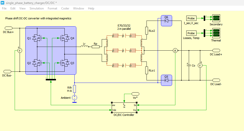
Figure 6: Phase shift DC-DC converter with integrated magnetics circuit in PLECS
Figure 6 presents the phase-shifted DC-DC converter with integrated magnetics implemented in PLECS. This converter provides galvanic isolation and voltage regulation between the DC link and the battery. The phase-shift control enables soft switching operation, reducing switching losses and improving efficiency. The integrated magnetics design enhances power density and reduces converter size.
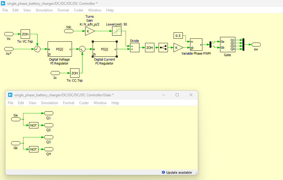
Figure 7: control logic of Phase shift DC-DC converter with its logic gate control
Figure 7 shows the control logic of the phase-shift DC-DC converter implemented using digital logic gates. The logic circuit generates appropriate gating signals for the full-bridge switches based on the phase-shift control strategy. This ensures proper timing coordination between switches, enabling efficient energy transfer and stable converter operation.
The converter utilizes a full-bridge switching topology consisting of four primary MOSFET switches driven by phase-shifted PWM signals. By varying the phase shift between the bridge legs rather than changing the switching frequency, the converter achieves efficient power regulation while maintaining soft-switching conditions over a wide operating range [13].
The resonant network, composed of resonant inductance and transformer leakage inductance, enables Zero Voltage Switching (ZVS) for the primary MOSFETs during most operating conditions. ZVS significantly reduces switching losses because the MOSFETs are turned on when the voltage across them approaches zero. Consequently, switching transitions become smoother, electromagnetic interference decreases, and converter efficiency increases substantially.
The high-frequency transformer performs multiple functions simultaneously. Besides providing electrical isolation required for battery charging safety, it also performs voltage transformation according to the required charging voltage. High-frequency operation permits the use of smaller magnetic components, contributing to reduced converter size and weight.
On the secondary side, rectifier diodes convert the transformer output into DC voltage. Output filter components remove residual switching ripple before supplying the battery load. The digital controller continuously monitors the output voltage and adjusts the bridge phase shift to maintain accurate voltage regulation despite changes in load demand.
The converter is designed to supply output voltages ranging from low charging levels up to approximately 120 V while delivering output power approaching 1.4 kW. During transient events such as reference voltage changes or sudden load variations, the converter exhibits rapid response with minimal overshoot, ensuring stable battery charging conditions.
D. Digital Control Strategy
A cascaded digital control strategy is implemented to coordinate both converter stages and achieve stable system operation. The control architecture consists of independent voltage and current feedback loops operating at different bandwidths. This hierarchical arrangement improves dynamic response while ensuring robust regulation under varying operating conditions.
For the AC/DC converter, the outer voltage loop regulates the intermediate DC-link voltage by comparing the measured capacitor voltage with the desired reference value. The resulting voltage error is processed using a digital proportional-integral controller equipped with an anti-windup mechanism. The anti-windup algorithm prevents excessive integral accumulation during transient saturation, thereby improving recovery time and preventing controller instability.
The output of the voltage controller generates the desired current reference for the inner current control loop. The measured input current is continuously compared with this reference, and the resulting error is processed by another PI controller that determines the required PWM duty ratio for both interleaved converter phases. Since the reference current is synchronized with the grid voltage, the converter naturally achieves high power factor operation.
The DC/DC converter employs an independent voltage regulation loop that continuously measures the battery output voltage. The controller adjusts the bridge phase shift according to the voltage error, ensuring accurate output regulation under varying charging conditions. Because both converters operate independently while exchanging energy through the regulated DC-link capacitor, the cascaded architecture effectively isolates disturbances occurring at either stage of the system.
Digital implementation also provides flexibility for future integration of advanced charging algorithms such as constant-current/constant-voltage charging, adaptive charging profiles, state-of-charge estimation, and battery management system communication without requiring significant hardware modifications.
E. Thermal Modeling
Thermal analysis is incorporated into the proposed PLECS model to evaluate the operating temperatures and reliability of the semiconductor devices. Power semiconductor losses generated during converter operation are converted into heat, causing junction temperatures to rise. Excessive junction temperatures accelerate semiconductor aging, increase conduction losses, and reduce converter lifetime.
The developed model includes detailed thermal descriptions for all primary MOSFET switches and output rectifier diodes. Thermal impedance networks obtained from manufacturer datasheets represent the heat transfer path from the semiconductor junction to the device case. These thermal models accurately estimate transient and steady-state junction temperatures during converter operation.
A common heat sink is connected to all semiconductor devices, allowing heat generated by individual switches and diodes to be dissipated collectively into the surrounding environment through a thermal resistance network. The ambient temperature serves as the thermal reference boundary condition throughout the simulation.
An additional advantage of the implemented thermal model is its capability to evaluate multiple semiconductor devices connected in parallel or series. The customized MOSFET model automatically scales thermal parameters according to the selected device configuration while assuming equal voltage and current sharing among parallel branches. This capability enables designers to investigate different power ratings without modifying the converter topology.
By integrating electrical and thermal simulations within a single environment, the proposed model provides valuable information regarding converter efficiency, device temperatures, heat sink performance, and overall system reliability. Such comprehensive analysis significantly reduces design iterations before experimental hardware implementation.
You can download the Project files here: Download files now. (You must be logged in).
III. Mathematical Modeling
The mathematical model of the proposed battery charger is developed to describe the dynamic behavior of the DC-link capacitor and the output power delivered to the battery load. Since the primary objective of this work is the system-level performance evaluation using PLECS rather than analytical controller design, only the essential equations governing the converter operation are presented.
A. DC-Link Voltage Dynamics
The intermediate DC-link capacitor acts as an energy buffer between the AC/DC power factor correction converter and the isolated DC/DC converter. During transient conditions, such as sudden load changes or output voltage reference variations, the capacitor temporarily stores or releases energy until both converter stages reach a new steady-state operating condition. The capacitor voltage variation can be expressed as [3][4].

where
- C_dc is the DC-link capacitance (F),
- V_dc is the DC bus voltage (V),
- I_PFC is the output current supplied by the AC/DC converter (A),
- I_Load is the input current drawn by the DC/DC converter (A), and
- (dVdc/dt) represents the rate of change of the DC-link voltage.
Equation (1) indicates that the capacitor voltage remains constant when the current supplied by the AC/DC converter equals the current consumed by the DC/DC converter. During rapid load increases, the DC/DC converter initially draws more current than supplied by the front-end converter, causing the capacitor voltage to decrease temporarily. Conversely, during load reduction, excess energy charges the capacitor until the control loops restore steady-state operation. The implemented digital PI controller continuously adjusts the AC/DC converter output current to regulate the DC-link voltage at the desired reference value of 300 V.
B. Output Power of the Battery Charger
The regulated output power delivered to the battery is determined by the product of the output voltage and output current, expressed as [3]

Where
- Po is the output power (W),
- Vo is the regulated output voltage (V), and
- Io is the battery charging current (A).
Equation (2) represents the instantaneous output power supplied to the battery. During the simulation, the controller regulates the output voltage from 96 V to 120 V while automatically adjusting the output current according to the connected load. As the charging voltage increases, the output power also increases until the converter reaches its rated power capability of approximately 1.4 kW. The digital controller maintains stable operation throughout these operating conditions while preserving accurate voltage regulation and converter efficiency.
The above mathematical expressions adequately describe the principal energy transfer mechanism of the proposed cascaded battery charger. Since the converter control strategy and magnetic components are implemented directly within the PLECS simulation environment, additional analytical derivations are unnecessary for evaluating system-level performance.
IV. PLECS Simulation Implementation
The proposed battery charger is modeled entirely in the PLECS simulation environment using electrical, control, thermal, and magnetic component libraries. PLECS provides an integrated platform for simultaneously analyzing converter operation, digital control algorithms, semiconductor losses, and thermal behavior. This unified modeling approach significantly reduces computational complexity while accurately representing the dynamic interaction between electrical and thermal domains.
The complete battery charger consists of two cascaded converter stages. The front-end stage implements an interleaved boost power factor correction converter connected directly to the single-phase utility supply through an input filter. The converter employs two identical boost phases operating with 180° phase displacement to minimize input current ripple and improve overall efficiency. Digital voltage and current controllers generate the pulse-width modulation signals required for both switching legs.
The second conversion stage is modeled as an isolated phase-shifted full-bridge resonant converter. The converter includes a high-frequency transformer, resonant components, output rectifier diodes, and output filtering elements. A dedicated digital controller continuously regulates the output voltage by adjusting the bridge phase shift according to the measured battery voltage.
The simulation also incorporates detailed thermal descriptions for all primary MOSFET switches and secondary rectifier diodes. Semiconductor thermal models include junction-to-case thermal impedance networks obtained from manufacturer specifications. All power devices share a common heat sink connected to the ambient environment through an equivalent thermal resistance. Consequently, electrical losses generated during converter operation are automatically converted into heat, allowing simultaneous observation of electrical and thermal performance.
The implemented model further supports multiple semiconductor devices connected in either parallel or series configurations. Automatic parameter scaling ensures proper representation of voltage sharing, current sharing, and thermal characteristics without requiring structural changes to the converter topology. Such flexibility enables convenient investigation of different power ratings and converter configurations during the design stage.
To evaluate converter performance under practical operating conditions, two transient disturbances are introduced during the simulation. Initially, the battery charging voltage is regulated at 96 V. At t = 0.2 s, the output voltage reference is increased to 120 V. This operating condition represents the transition between different battery charging levels commonly encountered in practical charging systems.
Later, at t = 0.35 s, the output load is doubled while maintaining the 120 V reference voltage. This disturbance evaluates the dynamic response of both converter stages and demonstrates the effectiveness of the cascaded control structure in maintaining stable operation despite rapid changes in power demand.
Throughout the simulation, the following quantities are continuously monitored:
- DC-link capacitor voltage
- Converter input voltage and current
- Output voltage
- Output current
- Output power
- Switching signals
- Semiconductor temperatures
- Thermal losses
- Grid current waveform
The recorded waveforms provide comprehensive information regarding voltage regulation, transient response, power quality, converter loading, and thermal performance.
The simulation results demonstrate that the proposed control strategy successfully regulates the DC-link voltage at 300 V while maintaining stable output voltage during reference changes and sudden load disturbances. Furthermore, the interleaved PFC converter maintains nearly sinusoidal input current synchronized with the utility voltage, confirming effective power factor correction throughout the operating range.
V. Simulation Results and Discussion
The proposed single-phase battery charger was evaluated using the PLECS simulation platform under different operating conditions to investigate its steady-state and transient performance. The simulation model integrates electrical, digital control, magnetic, and thermal domains, allowing comprehensive analysis of the converter behavior. The AC/DC converter regulates the intermediate DC-link voltage at 300 V while simultaneously performing power factor correction. The isolated phase-shifted DC/DC converter regulates the battery charging voltage and supplies power to the load under varying operating conditions.
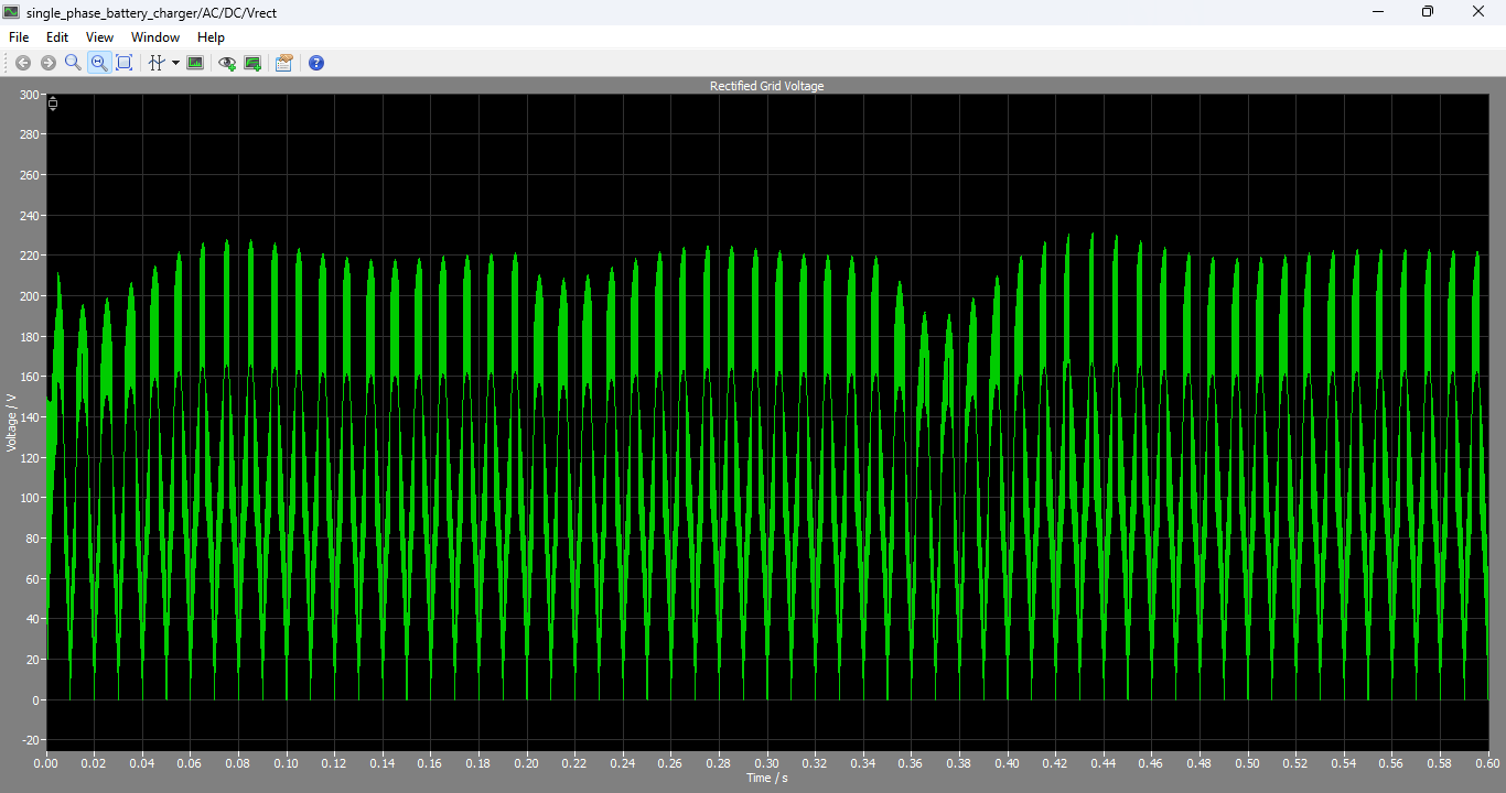
Figure 8: Rectified Grid sided voltage graph
Figure 8 shows the rectified grid-side voltage waveform after the AC/DC conversion stage. The waveform indicates successful rectification and regulation of the input AC voltage into a stable DC-link voltage. The controlled output ensures proper energy transfer to the subsequent DC/DC conversion stage.
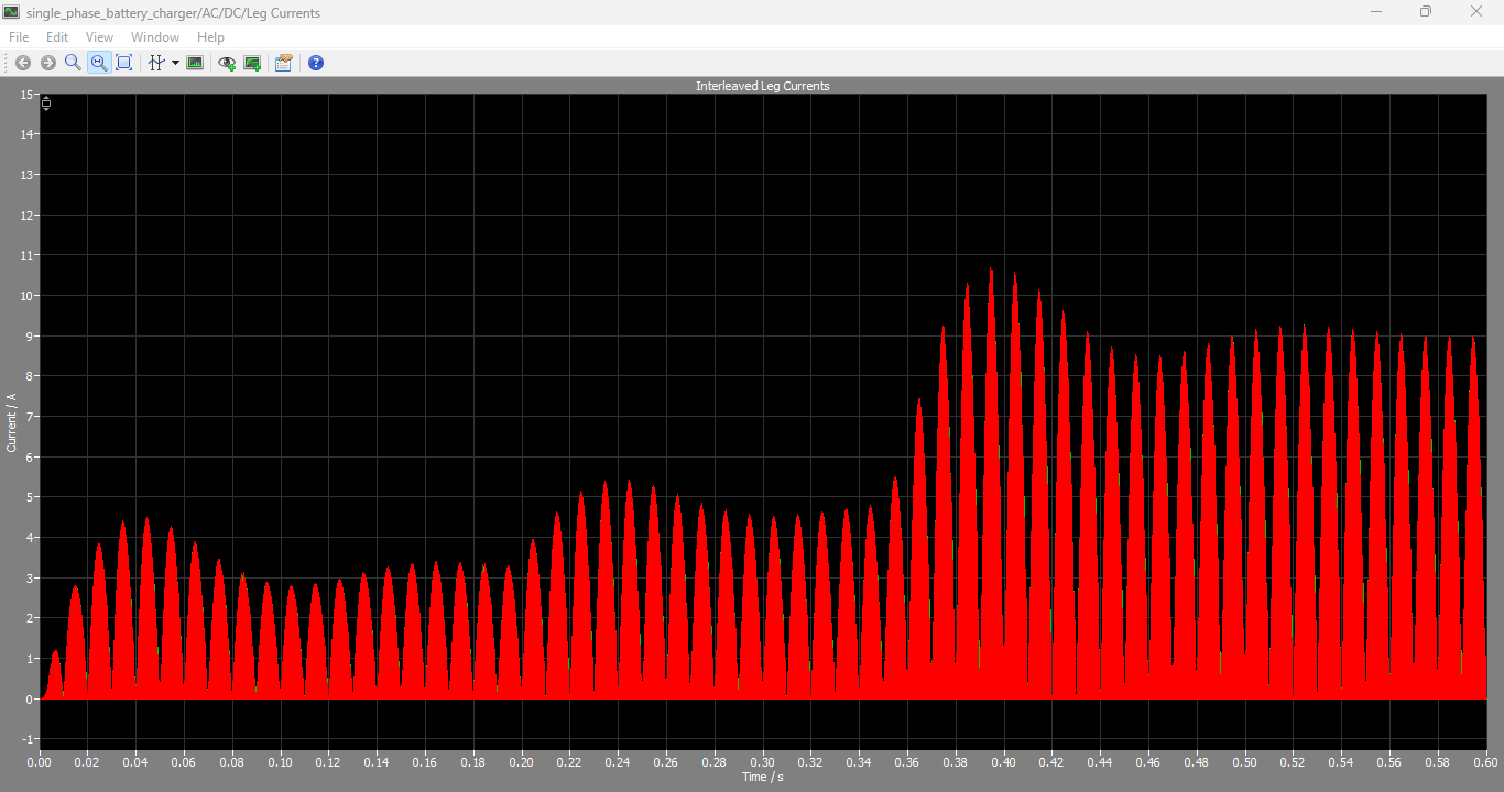
Figure 9: Interleaved Leg current graph
Figure 9 presents the interleaved leg currents of the AC/DC converter. The two interleaved phases operate with phase displacement, resulting in reduced current ripple and improved current sharing. This interleaving significantly enhances efficiency and reduces stress on semiconductor devices.
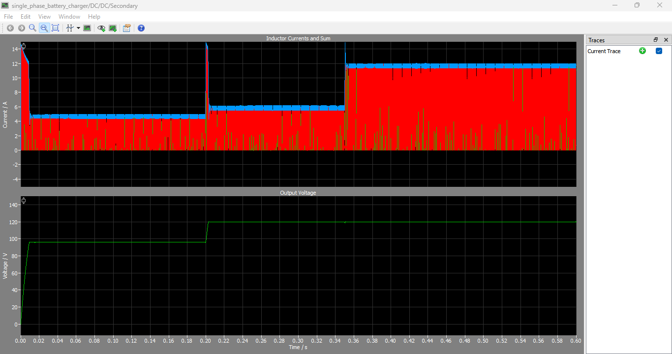
Figure 10: Secondary Sided currents and voltage graphs
Figure 10 illustrates the secondary-side voltage and current waveforms of the DC/DC converter. These waveforms confirm proper isolation and controlled energy transfer through the high-frequency transformer. The output is well regulated, showing stable charging behavior suitable for battery applications.
To assess the dynamic characteristics of the system, two operating disturbances were introduced during the simulation. Initially, the charger operates with an output voltage reference of 96 V. At 0.2 s, the reference voltage is increased to 120 V to evaluate the voltage tracking capability of the controller. Subsequently, at 0.35 s, the output load is doubled while maintaining the 120 V reference voltage to investigate load regulation and converter stability. The obtained simulation results verify that the proposed cascaded control strategy successfully maintains stable operation under both disturbances.
A. DC-Link Voltage Response
Fig. 11 illustrates the simulated DC-link capacitor voltage together with the corresponding reference voltage. The intermediate DC bus serves as the energy storage element connecting the AC/DC and DC/DC converter stages. Therefore, maintaining a constant DC-link voltage is essential for ensuring proper operation of the isolated converter.
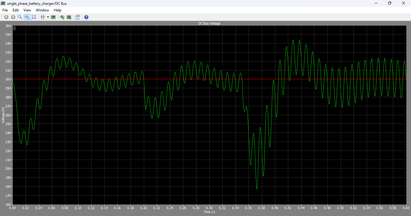
Figure 11: DC Bus Voltage output graph
You can download the Project files here: Download files now. (You must be logged in).
Figure 11 shows the DC-link voltage waveform of the battery charger system. The voltage is regulated at the desired reference value with minor transient variations during load changes. The control system effectively maintains voltage stability under dynamic operating conditions.
At the beginning of the simulation, the AC/DC converter rapidly charges the DC-link capacitor until the voltage reaches the desired reference value of 300 V. A short transient interval is observed during startup as the capacitor accumulates energy from the utility supply. After this initialization period, the voltage settles smoothly at the reference level with negligible steady-state error, demonstrating the effectiveness of the outer voltage regulation loop.
When the output voltage reference changes from 96 V to 120 V at 0.2 s, the DC/DC converter immediately demands additional power from the intermediate bus to satisfy the increased load requirement. As a result, the DC-link capacitor temporarily supplies the additional energy, causing a slight voltage sag. However, the digital PI controller quickly detects this deviation and increases the input power processed by the interleaved boost converter. Consequently, the capacitor voltage returns smoothly to the desired 300 V reference without excessive oscillations.
A similar behavior is observed at 0.35 s, when the load resistance is reduced, resulting in approximately twice the output current demand. Again, the capacitor initially compensates for the increased energy requirement, producing a temporary voltage drop. The front-end converter responds rapidly by increasing the input current drawn from the utility grid, thereby restoring the DC-link voltage within a short period.
The simulated waveform confirms that the cascaded voltage and current control loops provide excellent disturbance rejection capability. The transient voltage deviations remain relatively small, while the recovery time is sufficiently short for practical battery charging applications. Furthermore, no sustained oscillations or controller instability are observed throughout the simulation, indicating appropriate controller tuning and satisfactory closed-loop stability.
Overall, the DC-link voltage response demonstrates the effectiveness of the proposed control strategy in maintaining a stable intermediate energy storage stage under varying operating conditions.
B. Output Voltage, Current, and Power Characteristics
The simulated output voltage, charging current, and output power are presented in Fig. 12. These waveforms provide valuable insight into the dynamic performance of the isolated DC/DC converter and its digital control algorithm.
Initially, the converter regulates the battery charging voltage at approximately 96 V. The measured output voltage closely follows the reference signal, indicating accurate steady-state regulation. Since the converter employs a closed-loop voltage controller, only a very small steady-state error is observed.
At 0.2 s, the output voltage reference increases to 120 V. The controller immediately adjusts the phase shift of the full-bridge converter to increase the transferred power through the high-frequency transformer. Consequently, the output voltage rises smoothly toward the new reference value without excessive overshoot or oscillatory behavior.
Simultaneously, the charging current increases according to the new load requirements. The current waveform exhibits a controlled transient response before settling at its new operating point. The absence of large current spikes demonstrates that the controller effectively limits transient stress on both the semiconductor devices and the battery.
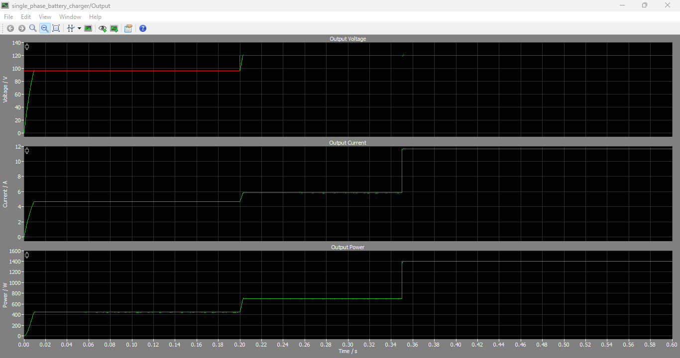
Figure 12: Output Voltage, Current and Power graphs of single phase battery charger
Figure 12 illustrates the output voltage, current, and power waveforms of the single-phase battery charger. The results demonstrate accurate voltage tracking, smooth current regulation, and stable power delivery up to the rated operating point. The system successfully maintains high efficiency and reliable charging performance.
The output power waveform reflects the combined variations in voltage and current throughout the simulation. During the initial operating interval, the converter delivers moderate output power corresponding to the 96 V charging condition. After the voltage reference increases, the delivered power rises proportionally as the converter supplies additional energy to the load.
At 0.35 s, the connected load is doubled while maintaining the 120 V output voltage reference. The digital controller automatically compensates for the increased current demand by transferring additional power from the DC bus. Although the output current increases significantly, the regulated output voltage remains nearly constant throughout the disturbance.
The maximum output power approaches approximately 1.4 kW, which corresponds to the rated operating condition of the proposed charger. Even under this high-power operating point, the converter maintains stable voltage regulation, confirming the effectiveness of the phase-shifted resonant topology and the implemented digital control strategy.
Another important observation is the smooth power transition throughout the entire simulation. Sudden power oscillations are effectively suppressed by the cascaded control loops, thereby reducing electrical stress on the converter components and improving battery charging quality.
The simulation results therefore demonstrate excellent load regulation, accurate voltage tracking, fast transient response, and reliable power delivery over the complete operating range.
C. Grid Voltage and Current Performance
The grid-side voltage and current waveforms are presented in Fig. 13. These waveforms evaluate the effectiveness of the interleaved boost converter in achieving power factor correction while minimizing harmonic distortion.
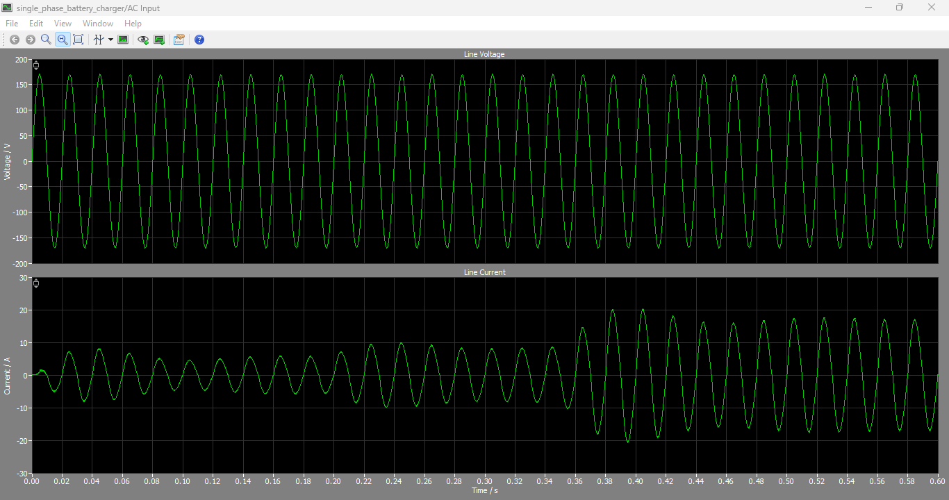
Figure 13: AC input line voltage and line current graphs
Figure 13 depicts the AC input line voltage and line current waveforms. The results demonstrate that the input current closely follows the sinusoidal grid voltage, confirming effective power factor correction. The near-unity power factor operation reduces harmonic distortion and improves overall grid compatibility of the battery charger.
The input voltage maintains the expected sinusoidal waveform corresponding to the single-phase utility source. More importantly, the input current closely follows the voltage waveform throughout the observed interval. Both waveforms exhibit nearly identical phase alignment, indicating that the converter operates with a power factor approaching unity.
The interleaved converter topology contributes significantly to this performance. Since the two boost converter phases operate with a 180° phase displacement, their ripple currents partially cancel each other. Consequently, the total input current contains considerably less ripple than that produced by a conventional single-phase boost converter.
The digital current controller continuously shapes the converter input current according to the instantaneous grid voltage. This synchronization minimizes reactive power exchange between the charger and the utility network while reducing low-order harmonic components.
Maintaining a high power factor provides several practical advantages. The utility source supplies primarily active power, resulting in improved energy utilization and reduced transmission losses. Furthermore, lower current harmonics decrease electromagnetic interference, improve compatibility with power quality standards, and reduce thermal stress within distribution equipment.
The simulated waveforms confirm that the proposed charger successfully satisfies the primary objective of the AC/DC converter, namely simultaneous DC-link voltage regulation and power factor correction.
D. Thermal and Overall System Performance
In addition to electrical performance, the developed PLECS model evaluates the thermal behavior of the semiconductor devices integrated within the battery charger. The thermal models associated with the MOSFET switches and output diodes continuously calculate junction temperatures based on the instantaneous power losses generated during converter operation.
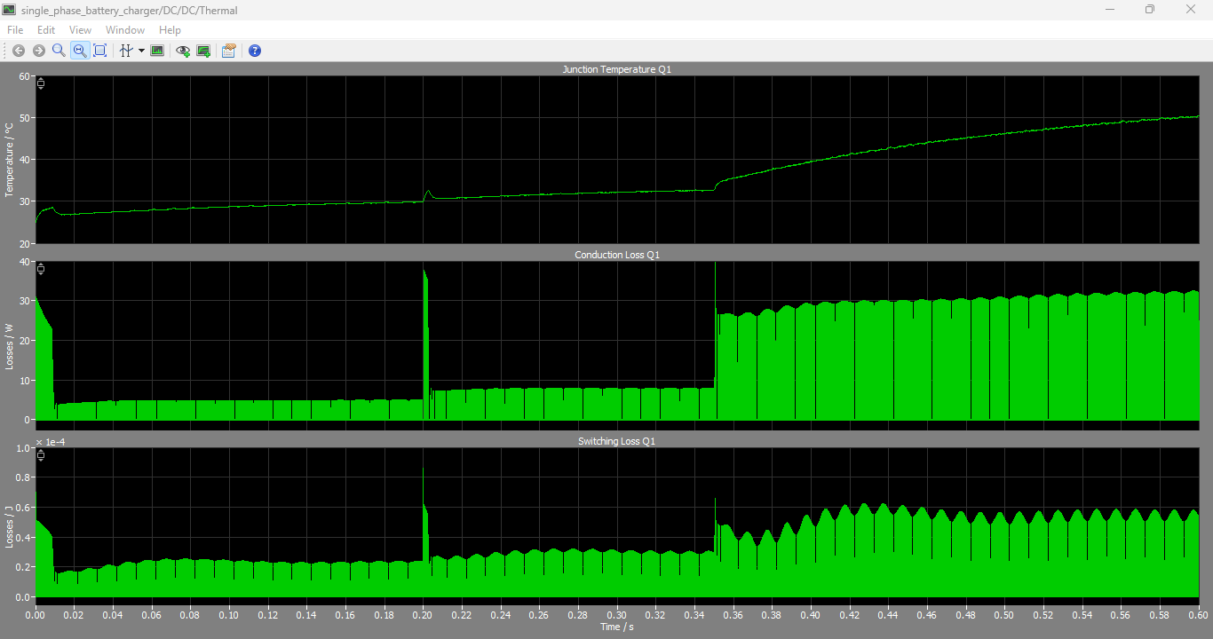
Figure 14: Thermal analysis including junction temperature and conduction Loss and switching loss output graphs
You can download the Project files here: Download files now. (You must be logged in).
Figure 14 presents the thermal analysis results, including junction temperature, conduction losses, and switching losses. The results show that semiconductor devices operate within safe thermal limits. The thermal model effectively captures power dissipation behavior and validates the reliability of the converter under rated conditions.
Throughout the simulation, heat generated by both the AC/DC and DC/DC converter stages is transferred through the thermal impedance networks toward the common heat sink before being dissipated into the surrounding environment. The integrated thermal analysis demonstrates that the selected semiconductor devices operate within acceptable temperature limits under rated operating conditions.
The interleaved PFC converter contributes to improved thermal performance by distributing the total input current between two switching legs. Since each MOSFET conducts only a portion of the total current, conduction losses are reduced and heat generation is more evenly distributed among the switching devices.
Similarly, the phase-shifted resonant converter benefits from soft-switching operation. Zero-voltage switching significantly decreases switching losses during transistor turn-on transitions, reducing both device temperature rise and overall converter losses. The resulting improvement in efficiency contributes directly to increased reliability and longer semiconductor lifetime.
The simulation also verifies that the common heat sink provides effective thermal coupling between the semiconductor devices. Temperature variations remain gradual throughout transient operating conditions, demonstrating that the thermal design is capable of handling temporary overload conditions without excessive junction temperature excursions.
Overall, the integrated electrical and thermal simulation confirms that the proposed battery charger achieves excellent voltage regulation, high conversion efficiency, rapid transient response, effective power factor correction, and satisfactory thermal performance. These characteristics make the proposed converter architecture highly suitable for medium- and high-power battery charging systems used in electric vehicles, renewable energy storage installations, industrial charging equipment, and smart-grid applications.
VI. Conclusion
This paper presented the modeling, control, and performance evaluation of a grid-connected single-phase battery charger developed using the PLECS simulation environment. The proposed charger employs a cascaded power conversion architecture consisting of an interleaved boost AC/DC power factor correction converter and an isolated phase-shifted resonant DC/DC converter. The two-stage topology combines high input power quality with accurate output voltage regulation, making it suitable for medium- and high-power battery charging applications.
A cascaded digital control strategy based on proportional-integral controllers was implemented to regulate both the intermediate DC-link voltage and the battery charging voltage. The front-end converter successfully maintained a regulated DC bus voltage of 300 V while simultaneously achieving near-unity power factor by shaping the input current to follow the utility voltage. The isolated DC/DC converter provided regulated output voltages up to 120 V with smooth transient performance during voltage reference changes and sudden load disturbances.
The simulation results demonstrated excellent steady-state and dynamic characteristics. During startup, the DC-link voltage rapidly converged to its reference value with negligible steady-state error. When subjected to output voltage step changes and increased load demand, the proposed control strategy maintained system stability while minimizing voltage deviations and recovery time. The output voltage accurately tracked the desired reference, and the output power increased smoothly to approximately 1.4 kW without excessive overshoot or oscillations. Furthermore, the interleaved converter effectively reduced input current ripple and maintained sinusoidal grid current, thereby improving power quality and reducing harmonic distortion.
An additional contribution of this work is the integration of thermal modeling within the electrical simulation. Detailed thermal descriptions of the MOSFET switches and output rectifier diodes enabled simultaneous evaluation of semiconductor temperatures and converter losses. The results confirmed that the common heat sink configuration and soft-switching characteristics of the phase-shifted resonant converter effectively limited device temperature rise, thereby improving converter reliability and expected operational lifetime.
The developed PLECS model provides a comprehensive platform for investigating converter performance before hardware implementation. Since electrical, magnetic, thermal, and control subsystems are integrated into a unified simulation environment, designers can efficiently evaluate system performance while minimizing development time and prototype iterations.
Future work may include experimental validation of the proposed charger using a laboratory prototype, implementation of advanced battery charging algorithms, incorporation of wide-bandgap semiconductor devices such as SiC or GaN switches, and development of intelligent battery management systems capable of adaptive charging based on battery state-of-charge and health estimation. These improvements can further enhance charging efficiency, reduce converter size, and increase the reliability of next-generation battery energy storage systems.
References
[1] V. Skanda and A. Nahar, Interleaved Power Factor Correction (IPFC) Using the dsPIC DSC, Microchip Technology Inc., Application Note AN1278, 2009.
[2] U. Badstuebner, J. Biela, B. Faessler, D. Hoesli, and J. W. Kolar, “An optimized 5 kW, 147 W/in³ telecom phase-shift DC-DC converter with magnetically integrated current doubler,” in Proc. IEEE Applied Power Electronics Conference and Exposition (APEC), Washington, DC, USA, 2009, pp. 21–27.
[3] N. Mohan, T. M. Undeland, and W. P. Robbins, Power Electronics: Converters, Applications and Design, 3rd ed. Hoboken, NJ, USA: Wiley, 2003.
[4] R. W. Erickson and D. Maksimović, Fundamentals of Power Electronics, 2nd ed. New York, NY, USA: Springer, 2004.
[5] D. M. Van de Sype, K. De Gusseme, F. M. L. L. De Belie, A. P. M. Van den Bossche, and J. A. Melkebeek, “Small-signal Laplace-domain analysis of uniformly sampled pulse-width modulators,” IEEE Trans. Power Electron., vol. 21, no. 3, pp. 757–765, May 2006.
[6] J. G. Cho, G. H. Rim, and F. C. Lee, “Zero-voltage and zero-current-switching full bridge PWM converter using secondary active clamp,” IEEE Trans. Power Electron., vol. 13, no. 4, pp. 601–607, Jul. 1998.
[7] J. W. Kolar and J. Miniböck, “The essence of three-phase PFC rectifier systems—Part I,” IEEE Trans. Power Electron., vol. 28, no. 1, pp. 176–198, Jan. 2013.
[8] D. Maksimović and R. Zane, “Small-signal discrete-time modeling of digitally controlled PWM converters,” IEEE Trans. Power Electron., vol. 22, no. 6, pp. 2552–2556, Nov. 2007.
[9] B. Jayant Baliga, Fundamentals of Power Semiconductor Devices. New York, NY, USA: Springer, 2008.
[10] Plexim GmbH, PLECS User Manual, Version 4.7.1, Zurich, Switzerland, 2023.
[11] H. Choi, M. Jang, and V. G. Agelidis, “Analysis and design of interleaved boost converters for power factor correction,” IEEE Trans. Power Electron., vol. 28, no. 2, pp. 987–998, Feb. 2013.
[12] L. Huber, B. T. Irving, and M. M. Jovanović, “Effect of valley switching and switching-frequency limitation on line-current distortions of DCM/CCM boundary boost PFC converters,” IEEE Trans. Power Electron., vol. 24, no. 2, pp. 339–347, Feb. 2009.
[13] R. Redl, N. O. Sokal, and L. Balogh, “A novel soft-switching full-bridge DC/DC converter: Analysis, design considerations and experimental results,” IEEE Trans. Power Electron., vol. 6, no. 3, pp. 408–418, Jul. 1991.
[14] M. H. Rashid, Power Electronics Handbook, 4th ed. Oxford, U.K.: Butterworth-Heinemann, 2018.
[15] F. Blaabjerg, U. Jaeger, and S. Munk-Nielsen, “Power losses in PWM-VSI inverter using NPT or PT IGBT devices,” IEEE Trans. Power Electron., vol. 10, no. 3, pp. 358–367, May 1995.
[16] J. Holtz, “Pulsewidth modulation for electronic power conversion,” Proc. IEEE, vol. 82, no. 8, pp. 1194–1214, Aug. 1994.
[17] B. Singh, B. N. Singh, A. Chandra, K. Al-Haddad, A. Pandey, and D. P. Kothari, “A review of single-phase improved power quality AC–DC converters,” IEEE Trans. Ind. Electron., vol. 50, no. 5, pp. 962–981, Oct. 2003.
[18] H. Akagi, E. H. Watanabe, and M. Aredes, Instantaneous Power Theory and Applications to Power Conditioning. Hoboken, NJ, USA: Wiley-IEEE Press, 2017.
[19] S. Buso and P. Mattavelli, Digital Control in Power Electronics, 2nd ed. San Rafael, CA, USA: Morgan & Claypool, 2015.
[20] IEEE Standards Association, IEEE Recommended Practice and Requirements for Harmonic Control in Electric Power Systems, IEEE Std. 519-2014, 2014.
[21] IEC, Electromagnetic Compatibility (EMC) – Limits for Harmonic Current Emissions (IEC 61000-3-2), International Electrotechnical Commission, Geneva, Switzerland, 2018.
[22] A. Emadi, A. Khaligh, Z. Nie, and Y. J. Lee, Integrated Power Electronic Converters and Digital Control. Boca Raton, FL, USA: CRC Press, 2009.
[23] K. Mainali and R. Oruganti, “High-frequency power converters for battery charging applications: A review,” IEEE Trans. Ind. Electron., vol. 61, no. 10, pp. 5464–5478, Oct. 2014.
[24] F. Musavi and W. Eberle, “Overview of wireless power transfer technologies for electric vehicle battery charging,” IET Power Electronics, vol. 7, no. 1, pp. 60–66, Jan. 2014.
[25] Y. Gu, Z. Lu, L. Hang, Z. Qian, and G. Huang, “Three-level LLC resonant converter for high-power battery charging systems,” IEEE Trans. Power Electron., vol. 30, no. 4, pp. 1860–1871, Apr. 2015.
You can download the Project files here: Download files now. (You must be logged in).










Responses