

Design and Thermal Performance Analysis of a Variable Frequency LLC Resonant DC–DC Converter Using PLECS Simulation

Author: Waqas Javaid
Abstract
High-efficiency isolated DC–DC converters have become indispensable in modern power electronic systems because of the increasing demand for compact, energy-efficient, and high-power-density converters. Among various resonant converter topologies, the LLC resonant converter has gained significant attention due to its ability to achieve soft-switching over a wide operating range while maintaining excellent efficiency and reduced electromagnetic interference (EMI). This paper presents the design, control, and thermal performance analysis of a variable frequency LLC resonant DC–DC converter developed in the PLECS simulation environment. The proposed converter employs a full-bridge inverter, an LLC resonant tank consisting of a resonant inductor, resonant capacitor, and transformer magnetizing inductance, followed by a high-frequency transformer and a full-wave diode rectifier to achieve isolated DC power conversion. Output voltage regulation is accomplished using a variable frequency control strategy based on a digital proportional–integral (PI) controller. The switching frequency is continuously adjusted according to load and voltage variations while maintaining zero-voltage switching (ZVS) for the primary-side MOSFETs. The thermal characteristics of silicon carbide (SiC) MOSFETs and Schottky diodes are also investigated using manufacturer-based thermal models integrated into PLECS. The simulation results demonstrate stable output voltage regulation, smooth startup through a soft-start algorithm, reduced semiconductor switching losses, and safe junction temperature operation under continuous switching conditions. Furthermore, the thermal analysis verifies that the proposed converter maintains reliable operation while benefiting from soft-switching characteristics that improve converter efficiency and reduce device stress. The presented simulation model provides an effective framework for the design and evaluation of high-frequency resonant converters intended for electric vehicle chargers, renewable energy systems, telecommunications power supplies, and industrial DC power conversion applications.
I. Introduction
The continuous development of renewable energy systems, electric vehicles, industrial automation, telecommunications equipment, and data centers has significantly increased the demand for efficient isolated DC–DC power converters capable of operating at high switching frequencies while maintaining excellent conversion efficiency [1], [2]. Conventional pulse-width modulation (PWM) converters experience substantial switching losses as switching frequency increases, limiting achievable power density and thermal performance [3]. Consequently, resonant power conversion techniques have become an attractive alternative because they substantially reduce switching losses while enabling compact magnetic components and improved overall efficiency.
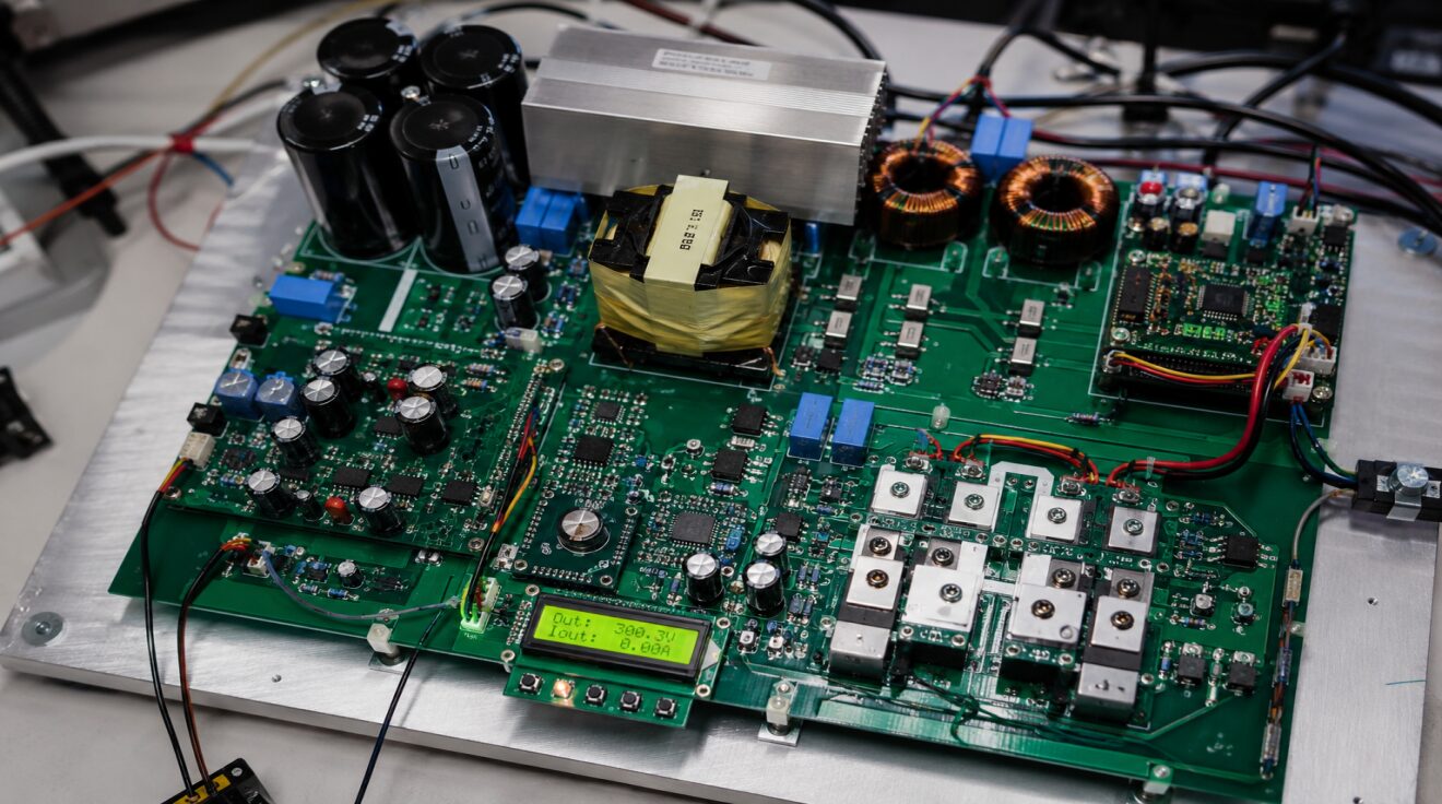
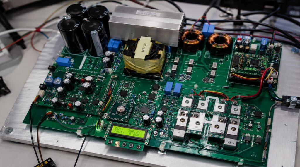
Figure A. Experimental Prototype of the Variable Frequency LLC Resonant DC–DC Converter
Figure A presents a practical laboratory prototype of the proposed variable frequency LLC resonant DC–DC converter designed for high-efficiency isolated power conversion. The hardware setup consists of a full-bridge silicon carbide (SiC) MOSFET inverter, an LLC resonant tank, a high-frequency isolation transformer, gate driver circuitry, control electronics, DC-link capacitors, and thermal management components mounted on a compact printed circuit board. The digital controller regulates the output voltage by varying the switching frequency while maintaining zero-voltage switching (ZVS) to minimize switching losses and improve overall efficiency. The integrated heat sink and power stage layout demonstrate the practical implementation of high-frequency resonant power conversion suitable for electric vehicle battery chargers, renewable energy interfaces, telecommunications power supplies, and other high-power-density industrial applications. This experimental configuration represents the real-world implementation corresponding to the PLECS simulation model investigated in this work.
Among different resonant converter topologies, the LLC resonant converter has emerged as one of the most widely adopted solutions for medium- and high-power isolated DC–DC conversion [1]. Unlike conventional hard-switched converters, the LLC converter utilizes a resonant network composed of a resonant inductor, resonant capacitor, and transformer magnetizing inductance to achieve efficient energy transfer. By operating near its resonant frequency, the converter enables zero-voltage switching (ZVS) of the primary-side MOSFETs and, under suitable operating conditions, zero-current switching (ZCS) of the secondary rectifier diodes [2]. These soft-switching characteristics significantly reduce switching losses, improve converter efficiency, decrease electromagnetic interference, and enhance long-term semiconductor reliability.
One of the most important features of LLC resonant converters is variable frequency control. Instead of varying the duty cycle, output voltage regulation is achieved by adjusting the switching frequency around the resonant frequency of the converter [3]. This operating principle enables efficient regulation over a wide load range while preserving soft-switching characteristics under varying operating conditions. Consequently, LLC converters have become the preferred choice for battery chargers, electric vehicle charging stations, server power supplies, aerospace systems, renewable energy interfaces, and industrial power converters [4].
Recent advances in wide-bandgap semiconductor devices, particularly silicon carbide (SiC) MOSFETs, have further enhanced the performance of LLC converters. Compared with conventional silicon devices, SiC MOSFETs offer lower switching losses, faster switching speed, higher breakdown voltage, and superior thermal capability [5]. These characteristics enable converters to operate efficiently at much higher switching frequencies while reducing cooling requirements and increasing power density.
Despite these advantages, designing an LLC converter remains challenging because of its nonlinear resonant characteristics and strong dependence on switching frequency, transformer parameters, and load conditions. Moreover, semiconductor thermal behavior plays a critical role in determining converter reliability and lifetime. Excessive junction temperature increases conduction losses, accelerates device degradation, and reduces overall system reliability [6]. Therefore, simultaneous electrical and thermal analysis has become an essential aspect of modern power converter design.
Simulation platforms have become indispensable tools for evaluating converter performance before hardware implementation. Among them, PLECS provides an integrated environment for electrical, magnetic, thermal, and control system modeling, enabling comprehensive analysis of converter operation under realistic conditions [5]. It supports accurate semiconductor loss calculation, variable-frequency PWM generation, thermal impedance modeling, and digital controller implementation, making it particularly suitable for high-frequency resonant converter analysis [7].
In this work, a complete LLC variable frequency resonant converter is developed and analyzed using the PLECS simulation platform. The proposed model consists of a full-bridge inverter, resonant tank, high-frequency transformer, diode rectifier, digital PI controller, variable-frequency PWM generator, and semiconductor thermal models. A soft-start strategy is incorporated to minimize startup stress, while closed-loop voltage regulation maintains the desired output voltage under changing operating conditions. Thermal models of SiC MOSFETs and Schottky diodes are integrated to evaluate semiconductor temperature rise and overall converter reliability.
The major contributions of this paper are summarized as follows:
- Development of a complete variable-frequency LLC resonant converter model using PLECS.
- Implementation of a closed-loop digital PI controller for output voltage regulation.
- Investigation of zero-voltage switching operation for improved converter efficiency.
- Integration of detailed semiconductor thermal models for junction temperature estimation.
- Evaluation of converter startup, steady-state operation, voltage regulation, and thermal behavior using comprehensive simulation results.
The remainder of this paper is organized as follows. Section II reviews recent developments in LLC resonant converter research. Section III describes the proposed converter topology and operating principle. Section IV presents the controller implementation and thermal modeling methodology. Section V discusses the simulation setup and performance evaluation, while Section VI concludes the paper.
II. Literature Review
Resonant power conversion has been extensively investigated over the past two decades due to its capability to improve efficiency while reducing switching losses in high-frequency converters. Erickson and Maksimovic [1] established the theoretical foundation of resonant converters by describing soft-switching techniques and their impact on converter efficiency. Their work demonstrated that LLC resonant converters offer significant advantages over conventional PWM converters by enabling zero-voltage switching across a wide operating range.
Several researchers have focused on improving converter efficiency through optimized resonant tank design. The selection of resonant inductance, resonant capacitance, and transformer magnetizing inductance directly affects voltage gain, circulating current, switching frequency range, and load regulation [2]. Proper resonant tank design allows converters to maintain high efficiency while minimizing conduction and switching losses over varying load conditions.
Digital control techniques have become increasingly popular for LLC converters because they provide greater flexibility than analog implementations. Texas Instruments introduced a digital LLC control strategy employing a two-pole two-zero PI controller for variable frequency regulation [3]. The controller adjusts the switching frequency according to output voltage error while maintaining stable closed-loop performance and preserving soft-switching operation.
The emergence of wide-bandgap semiconductor devices has significantly improved resonant converter performance. Silicon carbide MOSFETs exhibit lower switching energy, smaller output capacitance, and higher thermal conductivity than conventional silicon MOSFETs, enabling efficient operation at switching frequencies exceeding several hundred kilohertz [5]. These advantages have resulted in widespread adoption of SiC devices in electric vehicle chargers, renewable energy converters, aerospace power supplies, and industrial high-power applications.
Thermal analysis has become equally important in converter design because semiconductor lifetime strongly depends on junction temperature and thermal cycling. Modern simulation tools integrate electrical and thermal models, allowing simultaneous prediction of power losses, heat flow, and device temperature [4], [5]. Accurate thermal models enable designers to optimize heat sink dimensions, cooling systems, and switching strategies before hardware implementation.
Another important aspect concerns the modeling of switching losses under soft-switching operation. International Rectifier reported that conventional hard-switching loss estimation often overestimates switching losses because it neglects the recycling of energy stored in MOSFET output capacitance during zero-voltage switching [2]. Accurate loss estimation therefore requires detailed semiconductor loss models that incorporate both conduction and switching characteristics under practical operating conditions [8].
Recent studies have increasingly employed PLECS for integrated converter simulation because it combines electrical circuit analysis with digital control, magnetic modeling, and thermal simulation in a single environment [4], [5]. Compared with conventional simulation tools, PLECS provides computational efficiency while maintaining accurate prediction of semiconductor losses and junction temperatures under variable-frequency operation.
Although significant research has been reported on LLC resonant converters, relatively few studies simultaneously investigate electrical performance, digital frequency control, and detailed semiconductor thermal behavior within a unified simulation framework. Therefore, this work develops a comprehensive PLECS-based model that integrates variable-frequency control, soft-switching operation, detailed thermal modeling, and closed-loop voltage regulation to provide a practical design methodology for high-efficiency isolated DC–DC converters.
III. Proposed LLC Variable Frequency Resonant Converter
A. System Architecture
The proposed converter is developed using the PLECS simulation platform to investigate the electrical and thermal performance of an isolated LLC resonant DC–DC converter operating under variable-frequency control. As illustrated in Fig. 1, the converter consists of a full-bridge inverter, an LLC resonant tank, a high-frequency isolation transformer, a full-wave diode rectifier, an output filter, and a closed-loop digital controller. The complete system is designed to regulate the output voltage while maintaining soft-switching operation over a wide operating range.
A 200 V DC input source supplies the full-bridge inverter, which converts the input DC voltage into a high-frequency square-wave excitation. The inverter employs four silicon carbide (SiC) MOSFET switches arranged in an H-bridge configuration. These switches are driven with complementary gate pulses at a fixed duty ratio of 50%, while the switching frequency is continuously adjusted according to the controller output [9].
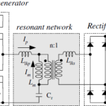
The inverter output is connected to the LLC resonant tank comprising the resonant inductor (Lr), resonant capacitor (Cr), and transformer magnetizing inductance (Lm). The resonant network performs three major functions: it shapes the current waveform, enables soft-switching operation, and transfers power efficiently from the primary side to the secondary side of the transformer. The transformer provides galvanic isolation while simultaneously adapting the voltage level according to the turns ratio.
On the secondary side, a full-wave diode rectifier converts the high-frequency AC voltage into pulsating DC. A capacitor filter suppresses the ripple components and supplies a regulated DC output voltage of approximately 300 V. The converter output is continuously monitored by a voltage sensing circuit whose signal is processed through a simplified analog-to-digital converter (ADC) before entering the digital controller.
Unlike conventional PWM converters, the proposed LLC converter regulates the output voltage by modifying the switching frequency rather than changing the duty cycle. This control technique preserves the resonant characteristics of the converter while ensuring high conversion efficiency and low switching losses under varying operating conditions [3].
B. Operating Principle
The LLC resonant converter transfers energy through the resonant interaction between the resonant inductance, resonant capacitance, and transformer magnetizing inductance. During each switching cycle, one diagonal pair of MOSFETs conducts while the opposite pair remains off. This operation generates an alternating square-wave voltage across the resonant tank.
When the switching frequency approaches the resonant frequency of the tank, the resonant current becomes nearly sinusoidal. The resonant current naturally charges and discharges the intrinsic output capacitances of the MOSFETs before each switching transition. Consequently, the corresponding anti-parallel diode begins conducting before the MOSFET is turned on, allowing zero-voltage switching (ZVS) to occur.
The elimination of turn-on switching losses represents one of the principal advantages of LLC converters. Since the MOSFET turns on when the voltage across the device is nearly zero, the switching energy dissipated during turn-on becomes negligible. This significantly improves converter efficiency, particularly at high switching frequencies where hard-switching losses become dominant [1], [2].
As the load changes, the controller adjusts the switching frequency to maintain the desired output voltage. Operating below resonance generally increases voltage gain, whereas operating above resonance decreases the converter gain. This frequency modulation technique enables smooth voltage regulation without changing the switching duty cycle.
The converter also incorporates a soft-start algorithm during startup. Instead of immediately applying the rated output voltage, the reference voltage gradually increases with a controlled slew rate. This approach limits inrush current, minimizes transformer magnetizing current, reduces semiconductor stress, and improves converter reliability during transient operation.
IV. Mathematical Modeling
The dynamic behavior of an LLC resonant converter is governed primarily by the resonant frequency of the LLC tank and the voltage regulation mechanism based on closed-loop control. Since this work emphasizes simulation and thermal analysis rather than analytical derivation, only two fundamental equations are presented.
A. Resonant Frequency
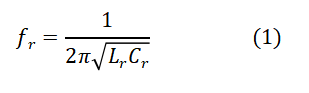
The resonant frequency of the LLC resonant tank is expressed as [1]
Where
- fr = resonant frequency (Hz),
- Lr = resonant inductance (H),
- Cr = resonant capacitance (F).
Equation (1) determines the natural operating frequency of the resonant tank. The controller continuously adjusts the switching frequency around this resonant frequency to regulate the converter output voltage while maintaining soft-switching operation. Operating close to the resonant frequency minimizes circulating current and maximizes conversion efficiency [1].
B. PI Voltage Controller
The digital controller generates the switching frequency command according to the voltage regulation error using the proportional-integral (PI) control law,

Where:
- u(t) = controller output,
- Kp = proportional gain,
- Ki = integral gain,
- e(t) = output voltage error,
- t = time.
The controller output is subsequently converted into a switching frequency command for the variable-frequency PWM generator. The proportional component provides rapid correction during transient disturbances, whereas the integral component removes steady-state voltage error, ensuring accurate output voltage regulation [3].
V. Digital Control Strategy
The proposed converter employs a digital closed-loop voltage controller to regulate the output voltage under varying operating conditions. The measured output voltage first passes through a sensing circuit represented by a low-pass transfer function that attenuates switching noise before analog-to-digital conversion.
The digitized voltage is compared with the reference voltage to generate the control error. The error signal is processed by a two-pole, two-zero digital PI controller that calculates the required switching frequency for the resonant converter. Instead of modifying the duty ratio, the controller varies the switching frequency while maintaining a constant 50% duty cycle for the full-bridge inverter.
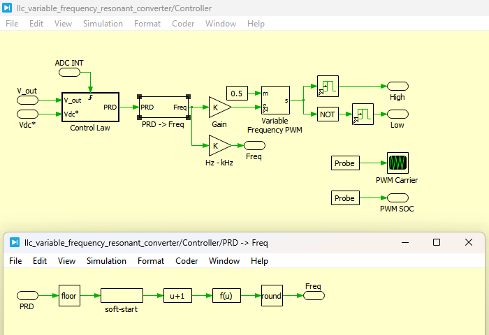
Figure 1: Controller designed for LLC variable frequency resonant converter in PLECS
Figure 1 presents the digital control architecture developed in the PLECS simulation environment for the LLC variable frequency resonant converter. The controller consists of a voltage sensing circuit, simplified Analog-to-Digital Converter (ADC), digital proportional–integral (PI) controller, frequency generation block, and variable-frequency PWM module. The measured output voltage is continuously compared with the reference voltage, and the resulting error signal is processed by the PI controller to generate the appropriate switching frequency command [10]. Unlike conventional PWM-controlled converters that regulate the output by varying the duty cycle, the proposed controller maintains a fixed 50% duty cycle while adjusting the switching frequency to achieve precise output voltage regulation. The controller also incorporates soft-start and voltage slew-rate limiting functions to reduce startup current, improve transient response, and minimize stress on the power semiconductor devices. This control strategy enables stable closed-loop operation, maintains zero-voltage switching (ZVS) over a wide operating range, and contributes to improved converter efficiency and thermal performance.
A variable-frequency PWM module generates complementary gate pulses for the four primary MOSFETs. Appropriate dead time is introduced between complementary switching transitions to ensure successful zero-voltage switching. During each switching cycle, the resonant current naturally discharges the output capacitance of the incoming MOSFET before turn-on, thereby minimizing switching losses.
To improve startup performance, a soft-start routine gradually increases the voltage reference after energization. This feature prevents excessive inrush current, avoids transformer core saturation, and reduces thermal stress on semiconductor devices. Furthermore, a voltage slew-rate limiter is incorporated to avoid abrupt reference changes during transient operating conditions, thereby improving system stability and output voltage regulation.
The digital implementation adopted in this study closely resembles practical embedded controller implementations used in industrial power supplies and electric vehicle chargers. The modular structure also facilitates future implementation using digital signal processors or microcontrollers.
You can download the Project files here: Download files now. (You must be logged in).
VI. Thermal Modeling of Power Semiconductors
Thermal management plays a vital role in ensuring the reliability and long-term operation of high-frequency power converters. Although silicon carbide MOSFETs exhibit excellent thermal capability compared with conventional silicon devices, excessive junction temperature can still reduce device lifetime and increase conduction losses.
In the proposed model, detailed thermal descriptions obtained from the semiconductor manufacturer are assigned to all four SiC MOSFETs in the primary full bridge and to the Schottky diodes used in the secondary rectifier. These thermal models include conduction loss characteristics, switching energy lookup tables, and thermal impedance networks representing the junction-to-case thermal path.
Unlike fixed-frequency converters, the LLC converter operates over a continuously changing switching frequency range. Therefore, the average conduction and switching losses cannot be calculated using conventional fixed-period averaging methods. Instead, PLECS employs variable impulse averaging and variable average calculation blocks that automatically adapt the loss calculation according to the instantaneous switching frequency. This approach improves the accuracy of power loss estimation throughout the operating range.
The generated semiconductor losses are transferred to a common heat sink model through thermal impedance networks. Heat is subsequently dissipated to the surrounding environment through an equivalent thermal resistance connected to the ambient temperature. This thermal network enables simultaneous calculation of device junction temperature, heat sink temperature, and overall thermal performance during transient and steady-state operation.
An important advantage of the proposed model is its ability to account for reduced switching losses resulting from zero-voltage switching. Since the MOSFET body capacitances are charged and discharged by the resonant current instead of dissipating energy during turn-on, the thermal stress experienced by the power devices is significantly reduced. Consequently, the simulated junction temperatures remain well within safe operating limits while maintaining high converter efficiency.
The integration of electrical and thermal simulation within a single PLECS environment provides valuable insight into converter performance and facilitates optimal semiconductor selection, heat sink design, and reliability assessment before hardware implementation.
VII. Simulation Results and Discussion
The proposed LLC variable frequency resonant converter was modeled and evaluated using the PLECS simulation platform. The simulation investigates the electrical performance, thermal behavior, soft-switching capability, and magnetic characteristics of the converter operating under closed-loop variable frequency control. The converter consists of a full-bridge inverter, an LLC resonant tank, a high-frequency transformer, a full-wave diode rectifier, and a digital PI controller responsible for output voltage regulation.
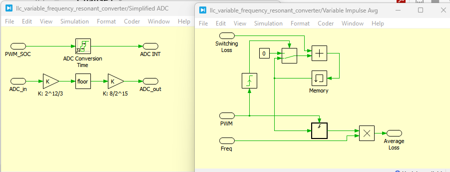
Figure 2: ADC and Variable Impulse response in PLECS Simulation
Figure 2 presents the Analog-to-Digital Converter (ADC) module together with the Variable Impulse Averaging subsystem implemented in the PLECS simulation model. The ADC block samples the filtered output voltage and converts the analog feedback signal into its corresponding digital representation for processing by the digital PI controller. The Variable Impulse Averaging block calculates the average switching losses over a variable switching period, making it particularly suitable for the LLC resonant converter where the switching frequency continuously changes during operation. Unlike conventional fixed-period averaging techniques, this approach accurately estimates the semiconductor switching losses under variable-frequency control, thereby improving the precision of thermal analysis and efficiency evaluation. The integration of these control and measurement blocks enables stable closed-loop voltage regulation while providing realistic loss calculation and thermal performance prediction throughout the converter’s operating range.
Initially, a DC input voltage of 200 V is applied to the converter. During startup, a soft-start algorithm gradually increases the voltage reference to eliminate excessive inrush current and reduce electrical stress on the semiconductor devices. Once the startup sequence is completed, the digital PI controller continuously adjusts the switching frequency to maintain the desired output voltage of approximately 300 V.
Unlike conventional hard-switched converters, the proposed converter operates with zero-voltage switching (ZVS), allowing the MOSFETs to switch at high frequencies with substantially reduced switching losses. Simultaneously, detailed semiconductor thermal models calculate conduction losses, switching losses, and junction temperatures throughout the simulation.
The following subsections discuss the performance of each simulation result.
A. Overall LLC Resonant Converter Model
Figure 3 illustrates the complete LLC variable frequency resonant converter developed in the PLECS simulation environment. The model integrates the power converter, resonant tank, transformer, digital controller, thermal models, voltage sensing circuit, and variable-frequency PWM generator into a unified simulation platform.
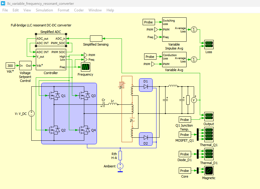
Figure 3: LLC Variable Frequency resonant converter Model in PLECS Simulation
The converter begins with a full-bridge inverter consisting of four SiC MOSFET switches. The bridge converts the DC input voltage into a high-frequency AC excitation for the resonant tank. The resonant network, composed of the resonant inductor, resonant capacitor, and transformer magnetizing inductance, transfers energy efficiently to the isolated secondary side. Following rectification and output filtering, the converter supplies a regulated DC output voltage.
The controller continuously monitors the output voltage and dynamically adjusts the switching frequency to compensate for voltage deviations caused by load or input disturbances. This integrated architecture provides accurate voltage regulation while preserving soft-switching operation and minimizing semiconductor losses.
B. Zero-Voltage Switching Performance
Figure 4 demonstrates the switching behavior of the primary-side MOSFETs during zero-voltage switching operation. The waveforms illustrate the relationship between device voltage and current during turn-on and turn-off transitions.
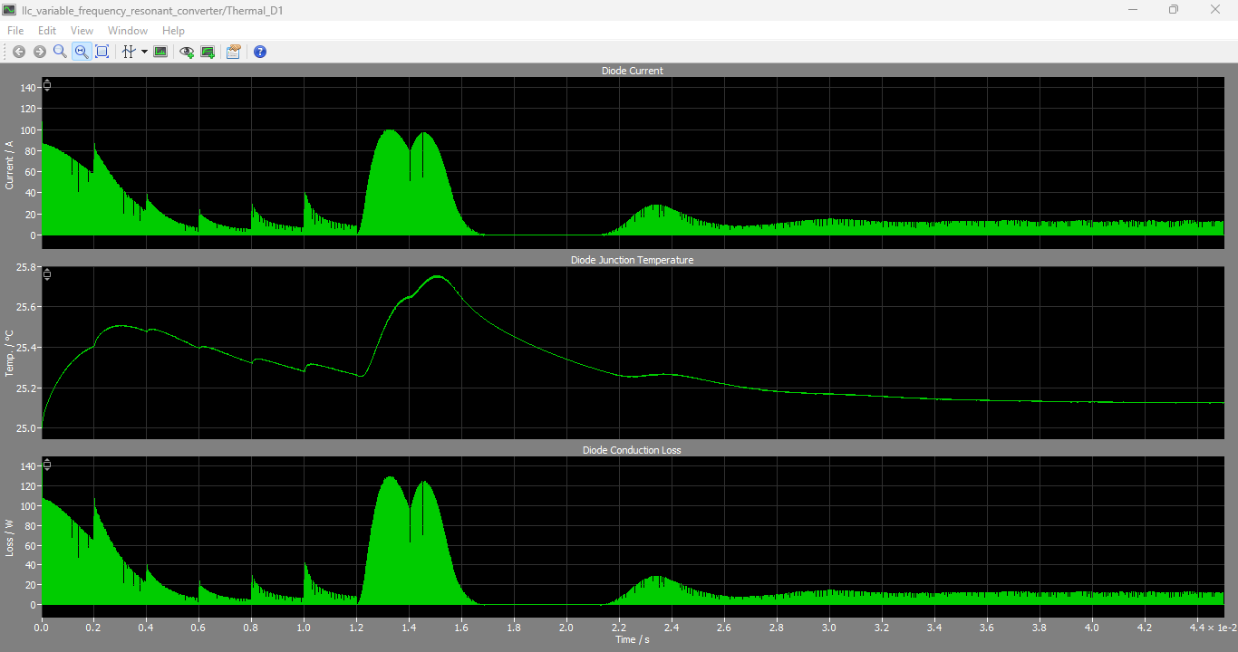
Figure 4: Diode Current, junction temperature and Diode conduction loss output graphs
Figure 4 presents the simulated diode current, junction temperature, and conduction loss characteristics of the secondary-side rectifier diodes during converter operation. The diode current waveform demonstrates stable current conduction through the rectifier during each switching cycle, ensuring efficient power transfer to the output load. The corresponding junction temperature increases gradually from ambient conditions before reaching a steady-state value, indicating effective thermal management under continuous operation. The conduction loss profile follows the diode current variation and remains within acceptable limits due to the use of high-performance SiC Schottky diodes with low forward voltage drop. These results confirm the reliable electrical and thermal performance of the output rectification stage.
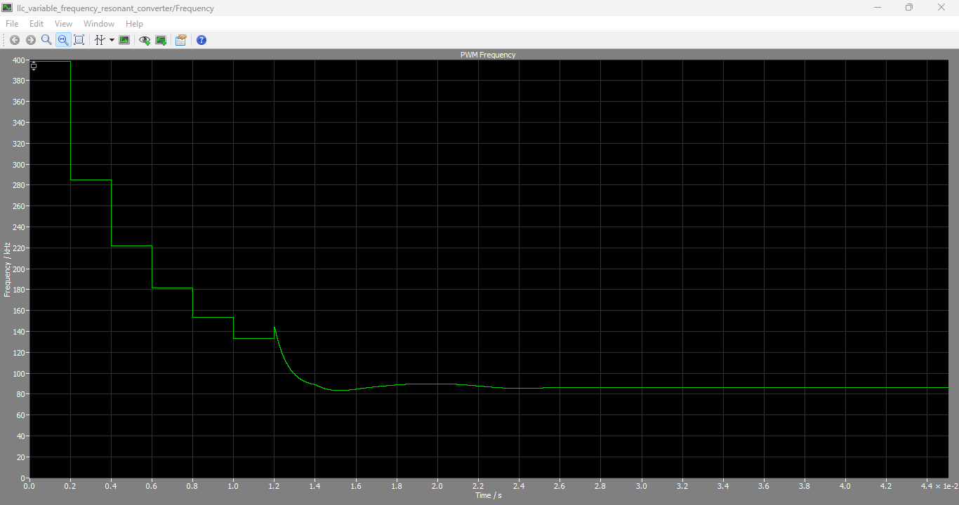
Figure 5: PWM Frequency output graph
Figure 5 illustrates the switching frequency generated by the variable-frequency PWM controller. Unlike conventional PWM techniques with fixed switching frequency, the proposed LLC resonant converter continuously adjusts its switching frequency to regulate the output voltage according to load and operating conditions. During startup, the controller gradually modifies the switching frequency as part of the soft-start strategy before settling near the desired operating point. The smooth frequency variation demonstrates the effectiveness of the digital PI controller in maintaining stable converter operation while preserving zero-voltage switching (ZVS) across the entire operating range.
Before each MOSFET is turned on, the resonant current naturally discharges the device output capacitance and forward-biases the anti-parallel body diode. Consequently, the voltage across the MOSFET becomes nearly zero before gate excitation is applied. Since the device begins conducting under zero-voltage conditions, turn-on switching losses become negligible.
During turn-off, however, current continues flowing through the device while voltage increases, resulting in moderate turn-off switching losses. Nevertheless, the elimination of turn-on losses represents a substantial reduction in total switching energy compared with conventional hard-switching converters.
The implementation of ZVS also decreases electromagnetic interference, lowers switching stress, and improves overall converter efficiency. These advantages become increasingly important at high switching frequencies where switching losses normally dominate converter performance.
C. Output Voltage Response During Startup
Figure 6 presents the transient response of the converter immediately after startup. The upper waveform illustrates the output voltage evolution, whereas the lower waveform shows the corresponding MOSFET junction temperature.
At the beginning of the simulation, the output voltage increases gradually due to the implemented soft-start algorithm. Instead of applying the full voltage instantaneously, the controller slowly ramps the reference voltage until the desired operating point is reached. This strategy effectively limits startup current and protects both the transformer and semiconductor devices.
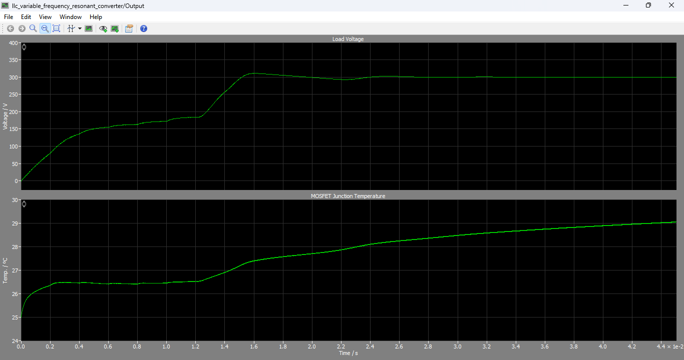
Figure 6: Load Voltage and MOSFET Junction Temperature
You can download the Project files here: Download files now. (You must be logged in).
Figure 6 presents the simulated output load voltage together with the junction temperature of the primary-side MOSFETs. The output voltage gradually increases during the startup interval because of the implemented soft-start algorithm and subsequently stabilizes around the reference value of 300 V with negligible steady-state error. Simultaneously, the MOSFET junction temperature increases smoothly as switching and conduction losses generate heat within the semiconductor devices. The temperature eventually reaches thermal equilibrium without exceeding the safe operating limits, demonstrating that the proposed converter maintains both excellent voltage regulation and reliable thermal performance during continuous operation.
After approximately 20 ms, the converter reaches its regulated output voltage of nearly 300 V with minimal overshoot and negligible steady-state error. The closed-loop digital controller demonstrates excellent transient performance by maintaining smooth voltage regulation throughout the startup process.
Simultaneously, the MOSFET junction temperature increases only slightly during converter energization. The limited temperature rise indicates that the soft-start algorithm successfully minimizes switching stress and prevents excessive power dissipation during transient operation.
Overall, the startup performance confirms the effectiveness of the proposed digital controller in achieving fast voltage regulation while maintaining safe thermal operating conditions.
D. MOSFET Junction Temperature Analysis
Figure 7 illustrates the long-term thermal response of the primary-side SiC MOSFETs. As converter operation continues, semiconductor power losses gradually increase the junction temperature until thermal equilibrium is established.
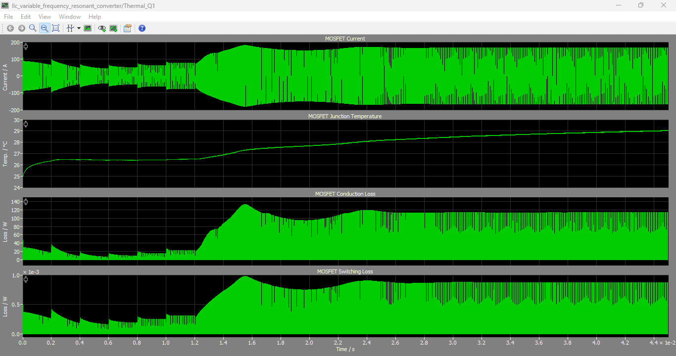
Figure 7: MOSFET Current, junction temperature, conduction loss and MOSFET Switching Loss output graphs
Figure 7 shows the electrical and thermal performance of the primary-side SiC MOSFETs, including the device current, junction temperature, conduction loss, and switching loss waveforms. The MOSFET current follows the resonant current profile of the LLC converter, enabling efficient energy transfer through the resonant tank. The junction temperature gradually rises as power is dissipated within the semiconductor before stabilizing under steady-state conditions. The conduction loss varies with the instantaneous device current, whereas the switching loss remains relatively low because the converter operates under zero-voltage switching (ZVS). The combined results verify that the proposed converter effectively minimizes semiconductor power losses while maintaining safe thermal operating conditions.
Initially, the junction temperature equals the ambient temperature. As switching and conduction losses accumulate, heat flows through the semiconductor package into the common heat sink before dissipating into the surrounding environment.
The simulation indicates that the junction temperature increases gradually without sudden thermal spikes or oscillations. Eventually, the temperature converges toward a stable steady-state value well below the maximum permissible junction temperature specified by the semiconductor manufacturer.
This stable thermal response demonstrates the effectiveness of combining zero-voltage switching with silicon carbide devices. Since switching losses remain relatively low throughout converter operation, thermal stress on the MOSFETs is significantly reduced. Consequently, the converter achieves improved reliability, extended semiconductor lifetime, and reduced cooling requirements.
The results also verify the accuracy of the integrated thermal models employed within the PLECS simulation environment, allowing realistic prediction of device operating temperatures before experimental implementation.
E. Transformer Magnetic Characteristics
Figure 8 illustrates the simulated B–H characteristic of the high-frequency transformer core used in the LLC resonant converter.
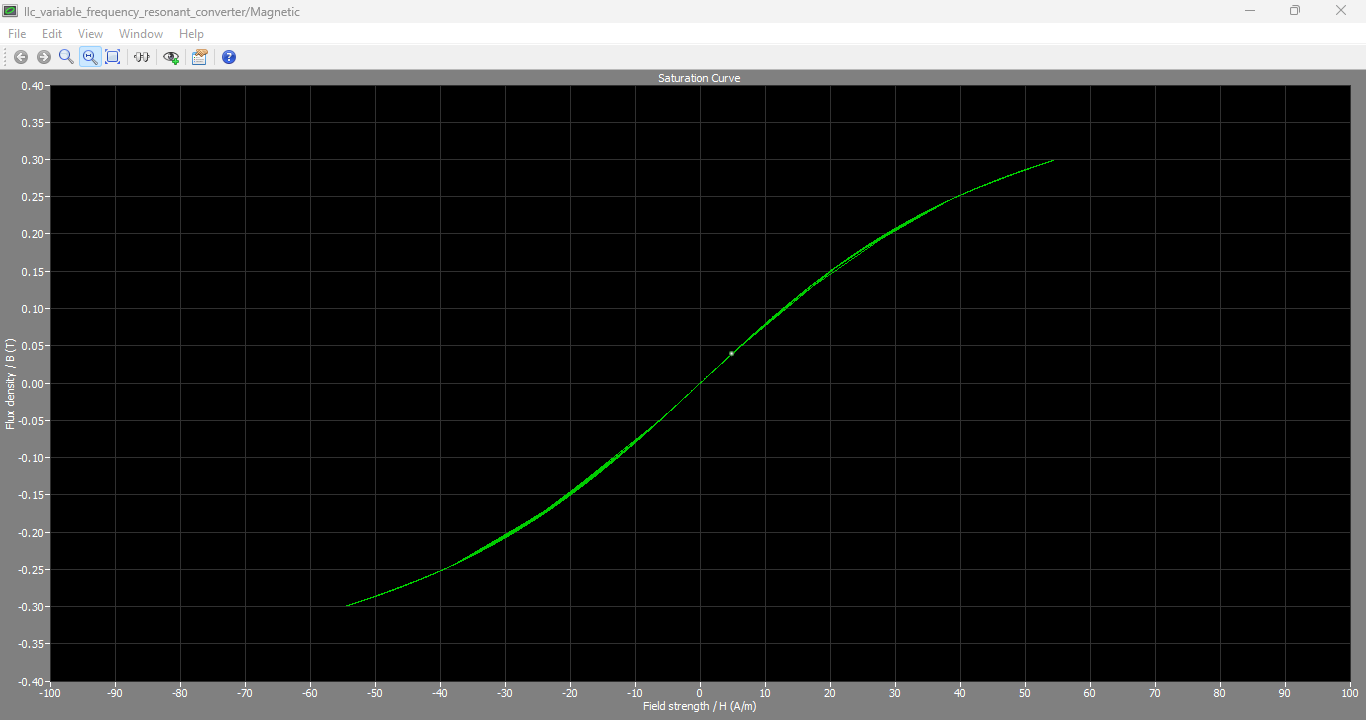
Figure 8: Saturation curve in transformer output graph
Figure 8 presents the simulated magnetic saturation (B–H) curve of the high-frequency transformer employed in the LLC resonant converter. The relationship between magnetic flux density and magnetic field intensity demonstrates that the transformer core operates within its linear magnetic region throughout the simulation. The absence of excessive magnetic saturation indicates that the selected transformer core material and resonant tank parameters are properly designed for high-frequency operation. Furthermore, the narrow hysteresis loop reflects low core losses and efficient magnetic energy transfer, thereby contributing to the overall high efficiency and stable operation of the proposed resonant converter.
The magnetic flux density varies almost symmetrically with respect to the magnetic field intensity, indicating balanced transformer excitation during converter operation. The operating point remains well within the linear region of the magnetic material, avoiding excessive magnetic saturation.
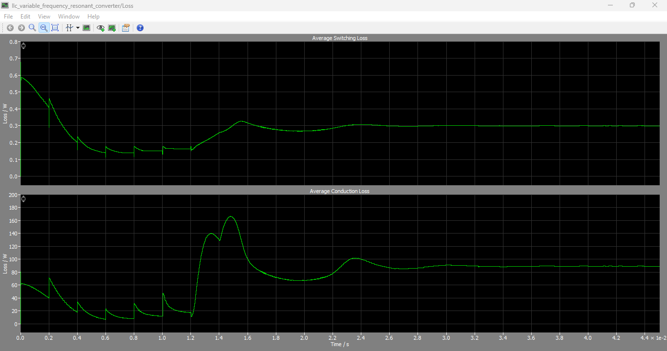
Figure 9: Average Switching and conduction loss
You can download the Project files here: Download files now. (You must be logged in).
Figure 9 illustrates the average switching losses and conduction losses of the semiconductor devices in the proposed LLC resonant converter under variable-frequency operation. The results are obtained using PLECS variable averaging techniques, which accurately capture power dissipation behavior over a non-constant switching period. The conduction loss component varies according to the instantaneous current flowing through the MOSFETs and diodes, while the switching loss component remains significantly reduced due to the zero-voltage switching (ZVS) operation of the converter. The combined average loss profile demonstrates that conduction losses dominate at higher load conditions, whereas switching losses remain relatively low across the operating range. This confirms the effectiveness of the resonant soft-switching strategy in minimizing high-frequency switching dissipation and improving overall converter efficiency and thermal performance.
The relatively narrow hysteresis loop indicates low core losses during high-frequency operation. Since magnetic saturation does not occur, the transformer operates efficiently throughout the simulated operating range while maintaining stable energy transfer between the primary and secondary windings.
Proper transformer design is essential in LLC converters because excessive core saturation increases magnetizing current, reduces efficiency, generates additional heat, and may eventually damage the converter. The simulated B–H curve confirms that the selected magnetic parameters satisfy the design requirements and support stable resonant operation.
F. Overall Converter Performance Evaluation
The simulation results collectively demonstrate the effectiveness of the proposed LLC variable frequency resonant converter under closed-loop operation. The digital controller accurately regulates the output voltage by varying the switching frequency while maintaining a constant duty ratio for the full-bridge inverter.
The implementation of zero-voltage switching substantially reduces semiconductor switching losses, allowing high-frequency operation without excessive temperature rise. The integrated thermal models indicate that all power semiconductor devices operate safely within their thermal limits throughout both transient and steady-state conditions.
Furthermore, the soft-start algorithm effectively suppresses startup current, improves converter reliability, and minimizes electrical stress on both the resonant tank and the transformer. The transformer magnetic analysis confirms stable magnetic operation without saturation, ensuring efficient energy conversion.
Overall, the proposed PLECS model provides a realistic representation of practical LLC resonant converter operation and serves as an effective platform for converter design optimization, controller development, thermal analysis, and semiconductor evaluation before hardware implementation.
VIII. Performance Summary
The proposed converter exhibits several important performance advantages:
- Accurate closed-loop regulation of the 300 V output voltage using variable-frequency control.
- Successful implementation of zero-voltage switching that minimizes MOSFET turn-on losses.
- Stable transient response with negligible overshoot during converter startup.
- Effective soft-start operation that limits inrush current and semiconductor stress.
- Safe semiconductor junction temperatures under continuous operation due to detailed thermal modeling.
- Stable transformer magnetic performance without evidence of core saturation.
- High suitability for high-frequency isolated DC–DC applications including electric vehicle battery chargers, renewable energy interfaces, telecom power supplies, industrial power systems, and data-center power conversion.
The simulation results demonstrate that the proposed LLC resonant converter achieves an excellent balance between electrical efficiency, thermal reliability, voltage regulation accuracy, and soft-switching performance, making it an attractive solution for modern high-efficiency isolated power conversion systems.
IX. Conclusion
This paper presented the design, simulation, and thermal performance evaluation of a variable frequency LLC resonant DC–DC converter using the PLECS simulation platform. The proposed converter integrates a full-bridge inverter, LLC resonant tank, high-frequency isolation transformer, full-wave diode rectifier, digital PI controller, and detailed semiconductor thermal models into a unified simulation framework. The use of variable frequency control enables accurate output voltage regulation while preserving the soft-switching characteristics of the converter over a wide operating range.
Unlike conventional hard-switched converters, the LLC topology achieves zero-voltage switching (ZVS) of the primary-side SiC MOSFETs, thereby significantly reducing switching losses and improving overall conversion efficiency. The digital PI controller continuously adjusts the switching frequency according to the output voltage error, ensuring stable closed-loop operation with fast transient response and negligible steady-state error. The implemented soft-start algorithm further enhances converter reliability by limiting startup current and reducing electrical stress on the resonant components and semiconductor devices.
A comprehensive thermal analysis was also performed using manufacturer-based thermal models integrated into PLECS. The simulation results demonstrated that the semiconductor junction temperatures increase gradually and stabilize within safe operating limits during continuous operation. The reduced switching losses achieved through soft-switching contribute directly to lower thermal stress, improved converter reliability, and potentially longer semiconductor lifetime.
The magnetic analysis of the high-frequency transformer confirmed stable operation without core saturation, indicating that the selected resonant parameters provide efficient energy transfer throughout the operating range. Furthermore, the integrated electrical, thermal, and control simulations demonstrate the capability of PLECS to accurately predict converter performance before hardware implementation.
Overall, the proposed LLC variable frequency resonant converter provides an efficient, reliable, and thermally robust solution for isolated DC–DC power conversion. Owing to its high efficiency, compact design, and excellent voltage regulation capability, the converter is well suited for modern applications such as electric vehicle battery chargers, renewable energy conversion systems, telecommunications power supplies, industrial automation, aerospace electronics, and high-density data center power systems.
Future work may include hardware implementation of the converter, experimental validation of the simulation results, optimization of resonant tank parameters under varying load conditions, advanced digital control techniques such as adaptive or predictive control, and efficiency comparison with other isolated converter topologies under identical operating conditions.
References
[1] R. W. Erickson and D. Maksimović, Fundamentals of Power Electronics, 2nd ed. New York, NY, USA: Springer, 2001.
[2] International Rectifier, “A More Realistic Characterization of Power MOSFET Output Capacitance (Coss),” Application Note AN-1001, 2005.
[3] Texas Instruments, “Digital Power Control Lab: LLC Resonant Converter,” Version 1.1, Jan. 2009.
[4] F. Prausse and M. Ahmed, “Efficient Microcontroller Peripheral Modeling with PLECS,” Bodo’s Power Systems, pp. 34–37, Jul. 2014.
[5] M. Ahmed and M. Luo, “LLC Resonant Converter Simulation Using PLECS,” Bodo’s Power Systems, pp. 30–33, Dec. 2014.
[6] R. Redl, “Power Electronics and Electromagnetic Compatibility,” IEEE Transactions on Power Electronics, vol. 15, no. 5, pp. 769–781, Sept. 2000.
[7] J. W. Kolar and J. Miniböck, “The Essence of Three-Phase PFC Rectifier Systems,” IEEE Transactions on Power Electronics, vol. 28, no. 1, pp. 176–198, Jan. 2013.
[8] N. Mohan, T. M. Undeland, and W. P. Robbins, Power Electronics: Converters, Applications and Design, 3rd ed. Hoboken, NJ, USA: John Wiley & Sons, 2003.
[9] D. G. Holmes and T. A. Lipo, Pulse Width Modulation for Power Converters: Principles and Practice. Hoboken, NJ, USA: John Wiley & Sons, 2003.
[10] B. K. Bose, Modern Power Electronics and AC Drives. Upper Saddle River, NJ, USA: Prentice Hall, 2002.
You can download the Project files here: Download files now. (You must be logged in).











Responses