

Design and Performance Analysis of a Two-Stage LED Driver Incorporating Boost Power Factor Correction and Flyback DC–DC Converter Using PLECS Simulation

Author: Waqas Javaid
Abstract
Light-emitting diode (LED) technology has become the preferred solution for residential, commercial, and industrial lighting because of its high luminous efficiency, extended operational lifetime, and reduced energy consumption. Despite these advantages, LEDs require well-regulated current sources and high-quality power conversion systems to achieve reliable operation and comply with international power quality standards. Conventional single-stage LED drivers often encounter challenges such as poor power factor, increased harmonic distortion, and inadequate output voltage regulation. To overcome these limitations, this paper presents the design and performance evaluation of a two-stage LED driver consisting of a Boost Power Factor Correction (PFC) converter followed by an isolated Flyback DC–DC converter. The Boost converter shapes the input current to follow the supply voltage while maintaining a regulated DC bus voltage, whereas the Flyback converter provides galvanic isolation and accurate voltage regulation for the LED load. Analytical controller design based on the K-factor loop-shaping technique is employed to achieve stable dynamic performance and improved transient response. The complete system is implemented and analyzed using the PLECS simulation environment. Performance evaluation focuses on input current waveform quality, total harmonic distortion (THD), power factor improvement, output voltage regulation, and output current ripple. The proposed architecture demonstrates high conversion efficiency, excellent power quality, and reliable voltage regulation, making it suitable for modern solid-state lighting applications requiring compliance with international harmonic standards.
I. Introduction
The rapid advancement of semiconductor lighting technology has significantly transformed the lighting industry over the past two decades. Compared with incandescent and fluorescent lamps, light-emitting diodes (LEDs) provide substantially higher luminous efficacy, lower maintenance costs, reduced environmental impact, and considerably longer operational lifetimes. These characteristics have encouraged their widespread adoption in residential buildings, commercial facilities, industrial environments, automotive lighting, and street illumination systems [1].
Although LEDs possess numerous advantages, they are current-driven semiconductor devices that require carefully regulated electrical power. Small variations in operating current may lead to considerable changes in luminous intensity, junction temperature, and overall device lifetime. Consequently, an efficient LED driver is essential for ensuring stable illumination, maintaining electrical safety, and maximizing energy efficiency [2].
The increasing penetration of LED lighting has also introduced new challenges related to power quality. International standards, including IEC 61000-3-2 and IEEE harmonic recommendations, require electronic lighting equipment to minimize harmonic distortion and maintain a high input power factor. Traditional diode bridge rectifiers followed by bulk capacitors draw highly distorted input currents, resulting in increased harmonic content, reduced system efficiency, and additional stress on the electrical distribution network [3]. These undesirable effects motivate the integration of power factor correction (PFC) techniques into LED driver circuits.
Among various PFC topologies, the Boost converter operating in continuous conduction mode (CCM) is widely recognized for its simplicity, high efficiency, and capability to produce nearly sinusoidal input current. By appropriately controlling the inductor current, the Boost converter enables the input current to remain proportional to the instantaneous input voltage, thereby significantly improving the displacement and distortion power factors [4]. As a result, the AC supply experiences reduced harmonic pollution while the DC bus voltage remains well regulated.
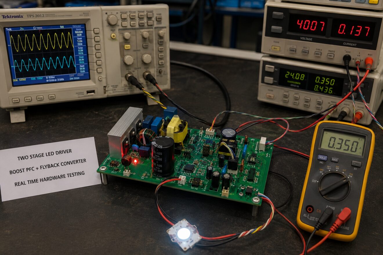
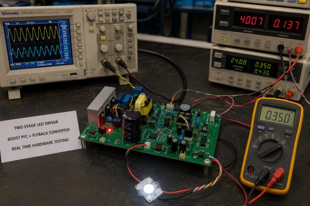
Figure A: Real-Time Hardware Testing Setup of the Proposed Two-Stage LED Driver
Figure A illustrates the experimental hardware setup used to validate the proposed two-stage LED driver under real-time operating conditions. The prototype consists of a Boost Power Factor Correction (PFC) stage integrated with an isolated Flyback DC–DC converter implemented on a custom-designed printed circuit board (PCB). The test bench includes a digital oscilloscope for monitoring the input and output waveforms, programmable DC power supplies, a digital multimeter for current measurement, and a high-power LED module serving as the load. During testing, the Boost converter regulates the intermediate DC-link voltage while shaping the input current to achieve a high power factor and low total harmonic distortion (THD). Simultaneously, the Flyback converter provides isolated and regulated power to the LED load, ensuring stable output voltage and constant current operation. The illuminated LED module confirms successful energy transfer through the complete converter system, while the measurement instruments verify the steady-state electrical characteristics and overall performance of the proposed hardware implementation.
While the Boost converter effectively performs AC–DC conversion and power factor correction, it is generally insufficient to satisfy the output regulation and isolation requirements of many LED applications. Therefore, an additional DC–DC conversion stage is frequently employed. Among available isolated converter topologies, the Flyback converter has become particularly attractive because of its simple structure, low component count, inherent galvanic isolation, and suitability for low- and medium-power applications [5]. The Flyback converter offers independent voltage regulation while allowing flexible transformer turns-ratio selection to accommodate different LED voltage ratings.
The combination of a Boost PFC front-end and a Flyback DC–DC converter has therefore emerged as one of the most practical solutions for high-performance LED power supplies. The first conversion stage improves input power quality and establishes a regulated intermediate DC bus, whereas the second stage supplies the LED array with a stable output voltage and current independent of variations in the AC mains voltage [6]. This two-stage architecture provides improved efficiency, better dynamic response, enhanced electrical isolation, and compliance with modern electromagnetic compatibility requirements.
Controller design plays a fundamental role in determining the performance of switching power converters. Conventional proportional-integral (PI) controllers are commonly employed; however, selecting appropriate controller parameters often requires repeated experimental tuning. Analytical controller design techniques provide more systematic solutions capable of ensuring adequate stability margins and desired bandwidths. Among these approaches, the K-factor loop-shaping method has gained considerable attention because it allows controller parameters to be calculated directly from the converter transfer function while satisfying specified crossover frequency and phase margin requirements [7]. Consequently, the resulting controller exhibits predictable transient performance with reduced overshoot and improved robustness against parameter variations.
Simulation has become an indispensable stage in the design of modern power electronic converters. Before hardware implementation, simulation platforms enable designers to verify converter operation, evaluate switching losses, analyze harmonic spectra, investigate transient conditions, and optimize controller parameters without the expense of physical prototyping. PLECS has established itself as a powerful simulation environment specifically developed for power electronic systems because it combines detailed semiconductor models, efficient numerical solvers, and flexible control system implementation within a unified framework [8].
This research investigates the design and simulation of a two-stage LED driver employing a Boost PFC converter and an isolated Flyback converter using PLECS. Particular emphasis is placed on improving input power quality while maintaining stable output voltage regulation under steady-state operating conditions. The proposed design incorporates analytical controller development based on the K-factor technique to achieve satisfactory dynamic characteristics. Simulation results evaluate important performance indicators including power factor, total harmonic distortion, output voltage ripple, output current ripple, and converter stability.
II. Literature Review
The development of high-performance LED drivers has attracted considerable research interest due to increasing global demand for energy-efficient lighting systems. Early LED power supplies primarily employed simple rectifier-capacitor circuits because of their low manufacturing cost and minimal component requirements. However, these circuits produced large harmonic currents, poor input power factors, and significant output voltage fluctuations, making them unsuitable for applications requiring compliance with international power quality standards [9].
Researchers subsequently introduced active power factor correction techniques to improve converter performance. The Boost PFC converter has become one of the most widely investigated topologies because it offers high efficiency, continuous input current, and relatively simple controller implementation [10]. Numerous studies have demonstrated that Boost PFC converters can achieve input power factors exceeding 0.99 while maintaining total harmonic distortion below regulatory limits.
To provide isolation and precise voltage regulation, Flyback converters have frequently been integrated with PFC stages in two-stage LED drivers. Their simple transformer structure, low component count, and cost-effectiveness make them particularly attractive for low- and medium-power lighting applications [11]. Recent investigations have further improved converter efficiency by employing optimized magnetic component design, digital control strategies, and advanced modulation techniques [12].
More recently, analytical controller design methods have been explored to replace empirical tuning procedures. The K-factor loop-shaping approach has received considerable attention because it enables systematic controller synthesis while guaranteeing specified stability margins and crossover frequencies [13]. Combined with simulation platforms such as PLECS, these methods provide an effective framework for designing reliable and efficient LED power conversion systems prior to hardware implementation.
III. Proposed Two-Stage Led Driver Architecture
The proposed LED driver consists of two cascaded power conversion stages designed to improve both input power quality and output voltage regulation. The first stage is a Boost Power Factor Correction (PFC) converter that converts the rectified AC supply into a regulated high-voltage DC bus while ensuring that the input current follows the sinusoidal shape of the supply voltage. The second stage is an isolated Flyback DC–DC converter that converts the intermediate DC bus voltage into a stable output suitable for driving a series-connected LED load.
Separating the power conversion process into two independent stages offers several advantages compared with single-stage converters. The Boost converter can be optimized solely for power factor correction, whereas the Flyback converter focuses on voltage regulation and electrical isolation. Consequently, each converter operates within a well-defined control objective, simplifying controller design while improving overall efficiency and reliability [14].
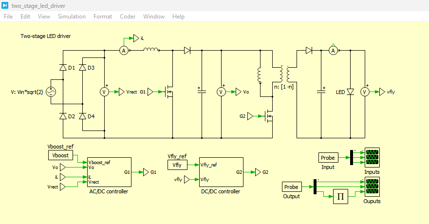
Figure 1: Proposed two-stage LED driver architecture in PLECS model.
You can download the Project files here: Download files now. (You must be logged in).
Figure 1 illustrates the overall architecture of the proposed LED driver. The AC mains supply is first rectified using a full-bridge diode rectifier. The rectified voltage is then processed by the Boost converter, producing a nearly constant DC-link voltage. Finally, the Flyback converter regulates the output supplied to the LED array.
A. Boost Power Factor Correction Converter
The Boost converter is one of the most commonly used active PFC topologies because it provides continuous input current and excellent harmonic performance. During operation, the converter shapes the input current such that it remains proportional to the instantaneous input voltage. Consequently, the converter draws nearly sinusoidal current from the utility grid while maintaining a regulated DC-link voltage.
The converter consists primarily of an input inductor, a controlled semiconductor switch, a fast recovery diode, and an output capacitor. Energy is temporarily stored within the inductor during the switch ON interval and transferred to the output capacitor during the OFF interval. By continuously adjusting the duty cycle through pulse-width modulation (PWM), the controller regulates both the input current waveform and the DC output voltage [4].
An outer voltage control loop compares the measured DC bus voltage with a predefined reference. The resulting voltage error is processed by a compensator to determine the required power transfer. An inner current control loop then forces the inductor current to track the generated current reference. This dual-loop configuration provides rapid dynamic response while maintaining excellent voltage regulation under varying load conditions.
The principal voltage conversion relationship of the Boost converter operating under ideal continuous conduction mode is expressed as
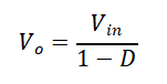
Where:
- Vo is the regulated DC output voltage,
- Vin represents the rectified input voltage,
- D denotes the converter duty ratio.
Equation (1) indicates that increasing the duty cycle results in a higher output voltage. Therefore, accurate duty-cycle control enables the converter to maintain a constant DC-link voltage despite fluctuations in the input supply voltage or output load demand [15].
B. Flyback DC–DC Converter
The Flyback converter serves as the second power conversion stage and provides galvanic isolation between the AC mains and the LED load. Owing to its relatively simple transformer structure and low component count, the Flyback converter is particularly suitable for low- and medium-power LED lighting applications [5].
Unlike conventional transformers, the Flyback transformer stores energy within its magnetizing inductance during the switch conduction interval. When the switch turns OFF, the stored magnetic energy is transferred to the secondary winding and delivered to the load. This operating principle enables simultaneous voltage conversion and electrical isolation using a single magnetic component.
A PWM controller continuously adjusts the duty ratio to regulate the output voltage. Since the converter operates from an already regulated DC-link voltage, the Flyback controller primarily compensates for load variations while maintaining constant LED operating conditions.
The transformer turns ratio significantly influences converter performance. Proper selection of the primary-to-secondary winding ratio allows the converter to satisfy different output voltage requirements without significantly increasing switching losses or magnetic component size.
C. LED Load Characteristics
Unlike resistive loads, LEDs exhibit highly nonlinear current-voltage characteristics. Small increases in forward voltage produce substantial increases in forward current. Consequently, constant-voltage supplies alone cannot guarantee safe LED operation.
The LED array considered in this study consists of multiple high-brightness LEDs connected in series to obtain the required illumination level. Since identical current flows through every device connected in series, brightness uniformity is improved while simplifying current regulation.
Temperature also affects LED electrical characteristics. As junction temperature increases, the forward voltage decreases while luminous efficiency gradually declines. Consequently, maintaining stable operating current through appropriate converter control improves both reliability and service life [16].
D. Operating Principle
The complete converter operates sequentially through two independent energy conversion stages.
Initially, the AC supply is rectified into pulsating DC. The Boost converter then processes this voltage while simultaneously correcting the input power factor. The resulting regulated DC bus supplies the Flyback converter.
The Flyback converter subsequently transfers energy through its high-frequency transformer and regulates the output voltage supplied to the LED array. Because each stage performs an independent function, controller interaction remains limited, improving both stability and dynamic performance.
The proposed architecture therefore combines excellent input power quality with accurate output voltage regulation, making it well suited for high-performance solid-state lighting systems.
IV. Controller Design and Simulation Methodology
A. Control Strategy
Reliable operation of switching power converters depends heavily on appropriate controller design. In the proposed LED driver, independent controllers are implemented for the Boost PFC converter and the Flyback converter to satisfy their respective control objectives.
The Boost converter employs a cascaded dual-loop control structure. The outer voltage loop regulates the intermediate DC-link voltage by comparing the measured output voltage with a predefined reference value. The voltage controller determines the amount of input power required to satisfy the load demand.
The output of the voltage controller is multiplied by the rectified input voltage waveform, producing a sinusoidal current reference. The inner current controller subsequently forces the inductor current to track this reference using PWM switching. This approach ensures that the input current remains nearly sinusoidal and in phase with the input voltage, thereby achieving a high power factor and reduced harmonic distortion [17].
The Flyback converter uses a single voltage feedback loop. The measured output voltage is continuously compared with the desired LED operating voltage. The resulting error signal is processed through a compensator that determines the PWM duty ratio required to maintain stable output regulation.
B. K-Factor Controller Design
To improve controller robustness, the compensators are designed using the K-factor loop-shaping technique rather than empirical tuning methods. The K-factor method allows controller parameters to be calculated analytically from the converter transfer function while satisfying predetermined crossover frequency and phase margin specifications.
This technique first evaluates the converter frequency response at the desired crossover frequency. The controller phase boost is then selected to achieve the required stability margin. Finally, controller gain and compensator pole-zero locations are calculated analytically, producing predictable transient performance without repeated trial-and-error adjustment.
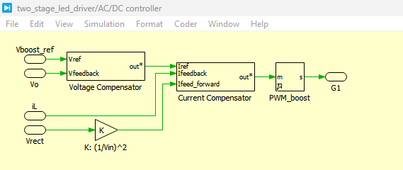
Figure 2: AC to DC controller Model in PLECS
Figure 2 presents the AC-to-DC controller implemented for the Boost PFC converter in the PLECS environment. The controller employs a cascaded dual-loop control strategy consisting of an outer voltage control loop and an inner current control loop. The voltage controller regulates the DC-link voltage, while the current controller shapes the input current to follow the rectified input voltage waveform, thereby improving the input power factor and reducing harmonic distortion.
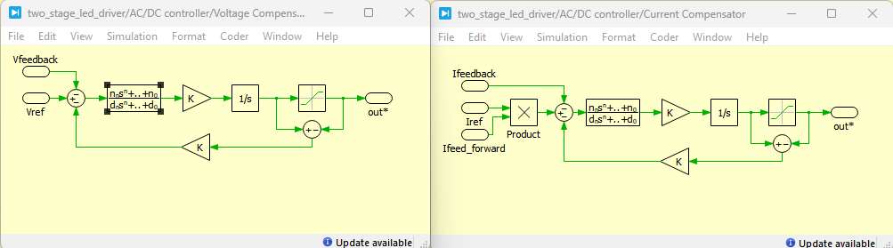
Figure 3: Voltage and Current Compensator Model in PLECS
You can download the Project files here: Download files now. (You must be logged in).
Figure 3 presents the voltage and current compensator models used within the Boost PFC control system. The compensators are designed based on the K-factor loop-shaping technique to achieve the desired crossover frequency and phase margin. The voltage compensator maintains a constant DC-link voltage, whereas the current compensator ensures accurate tracking of the reference current, resulting in stable converter operation, fast transient response, and improved overall control performance.
Compared with conventional tuning procedures, the K-factor method provides improved design consistency, enhanced stability margins, and superior dynamic response under varying operating conditions [13].
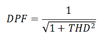
The distortion power factor associated with harmonic current is determined using
Where:
- DPF represents the distortion power factor,
- THD denotes the total harmonic distortion expressed in per-unit form.
Equation (2) demonstrates that lower harmonic distortion directly improves the distortion power factor. Consequently, minimizing input current harmonics through effective Boost PFC control significantly enhances the overall electrical performance of the converter [18].
C. PWM Generation
Pulse-width modulation provides the switching signals required by both power converters. High-frequency triangular carrier signals are continuously compared with the controller outputs to determine the appropriate switch duty ratios.
Changing the duty ratio regulates energy transfer through the converters while maintaining constant switching frequency. This simplifies filter design and enables accurate digital implementation within simulation software.
D. PLECS Simulation Model
The complete converter system is implemented using the PLECS simulation environment. Individual models are developed for the bridge rectifier, Boost converter, Flyback converter, PWM generators, feedback controllers, and LED load.
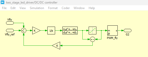
Figure 4: DC to DC controller Model in PLECS
Figure 4 presents the DC-to-DC controller developed for the Flyback converter in the PLECS simulation model. The controller continuously compares the measured output voltage with the reference voltage and adjusts the PWM duty cycle accordingly to regulate the output supplied to the LED load. This control strategy provides stable output voltage regulation, minimizes steady-state ripple, and maintains reliable operation under varying load conditions while ensuring efficient energy transfer through the isolated Flyback converter.
Simulation enables verification of converter performance before hardware implementation. Various operating quantities including input current, inductor current, DC-link voltage, output voltage, LED current, output power, and harmonic spectra are monitored throughout the simulation.
E. Performance Evaluation
Several performance indicators are analyzed to assess converter effectiveness. These include input power factor, total harmonic distortion, DC-link voltage stability, LED output voltage regulation, output current ripple, and transient response.
A high-quality LED driver should exhibit nearly sinusoidal input current, low harmonic distortion, stable DC-link voltage, minimal output ripple, and rapid recovery following load or input disturbances.
Simulation results demonstrate that the proposed two-stage architecture successfully achieves these objectives while maintaining stable operation throughout the entire simulation interval. The combination of Boost PFC control and Flyback voltage regulation provides an effective solution for modern high-efficiency LED lighting applications.
V. Simulation Results and Discussion
The proposed two-stage LED driver was modeled and analyzed using the PLECS simulation environment to evaluate its steady-state performance, power quality, and output voltage regulation. The complete simulation model included an AC voltage source, a full-bridge rectifier, a Boost power factor correction converter, an isolated Flyback converter, PWM control circuits, and a nonlinear LED load. The controllers were designed using the K-factor method discussed in the previous section to ensure stable operation and satisfactory transient response.
The simulation was performed under nominal operating conditions, and the converter was allowed to reach steady state before performance measurements were recorded. Several electrical quantities including input voltage, source current, inductor current, DC-link voltage, LED output voltage, output current, and output power were monitored throughout the simulation period.
A. Input Performance Analysis
The first stage of the converter is responsible for improving the quality of the current drawn from the AC supply. Figure 5 illustrates the input voltage waveform together with the corresponding source current. It can be observed that the input current closely follows the sinusoidal profile of the supply voltage, indicating successful operation of the Boost PFC controller.
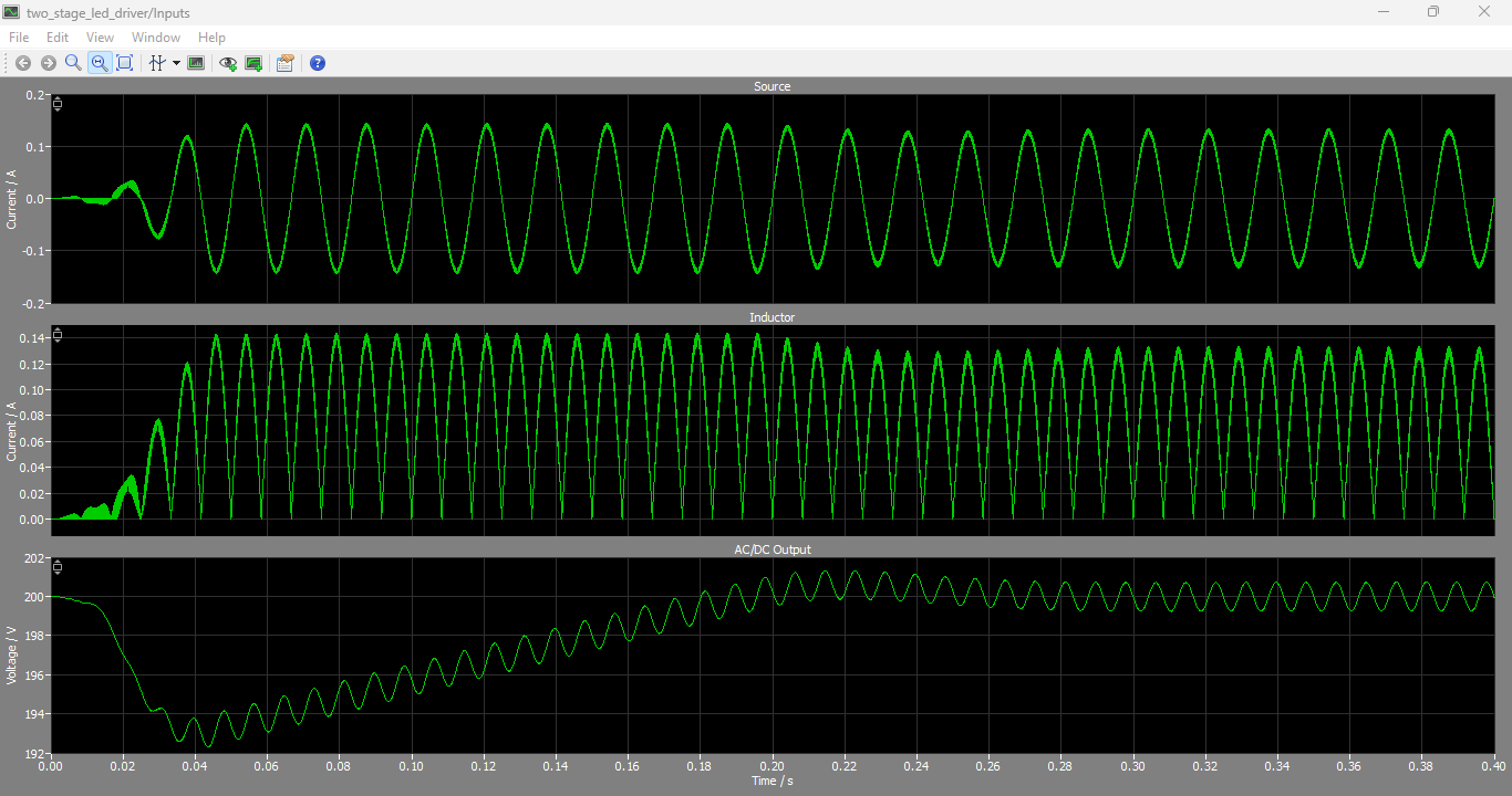
Figure 5: Input voltage, source current, and Boost inductor current.
The nearly identical phase relationship between the input voltage and current demonstrates that the converter operates with a very high power factor. Since the current waveform contains very little harmonic distortion, the converter satisfies the primary objective of active power factor correction.
The inductor current remains continuous throughout the switching cycle, which is expected because the converter operates in continuous conduction mode. Continuous current operation reduces switching stress, minimizes current ripple, and improves converter efficiency.
B. DC-Link Voltage Regulation
Figure 6 presents the regulated DC-link voltage generated by the Boost converter. Following the initial startup transient, the output voltage rapidly converges to its reference value with only a small overshoot. The controller effectively compensates for variations occurring during converter startup and subsequently maintains a nearly constant intermediate bus voltage.
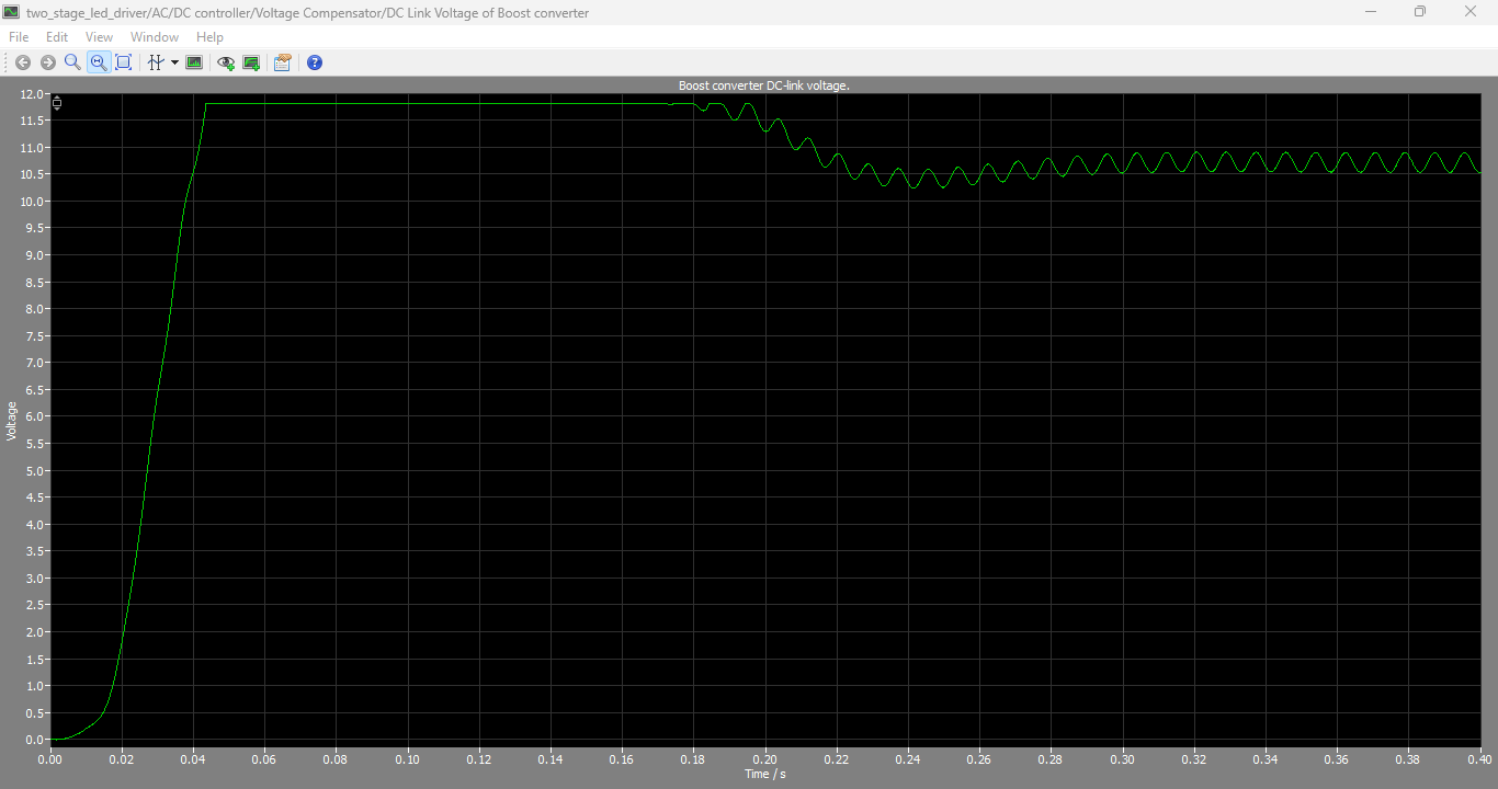
Figure 6: Boost converter DC-link voltage.
Stable DC-link voltage is essential because it serves as the input supply for the Flyback converter. Voltage fluctuations at this stage could directly influence the regulation capability of the second conversion stage. The simulation demonstrates that the designed voltage controller maintains excellent regulation throughout steady-state operation.
C. Flyback Converter Output Performance
The regulated DC-link voltage generated by the Boost converter is supplied to the Flyback converter, which provides galvanic isolation and regulates the electrical power delivered to the LED load. Figure 7 presents the steady-state output characteristics of the Flyback converter, including the LED output voltage, output current, and output power.
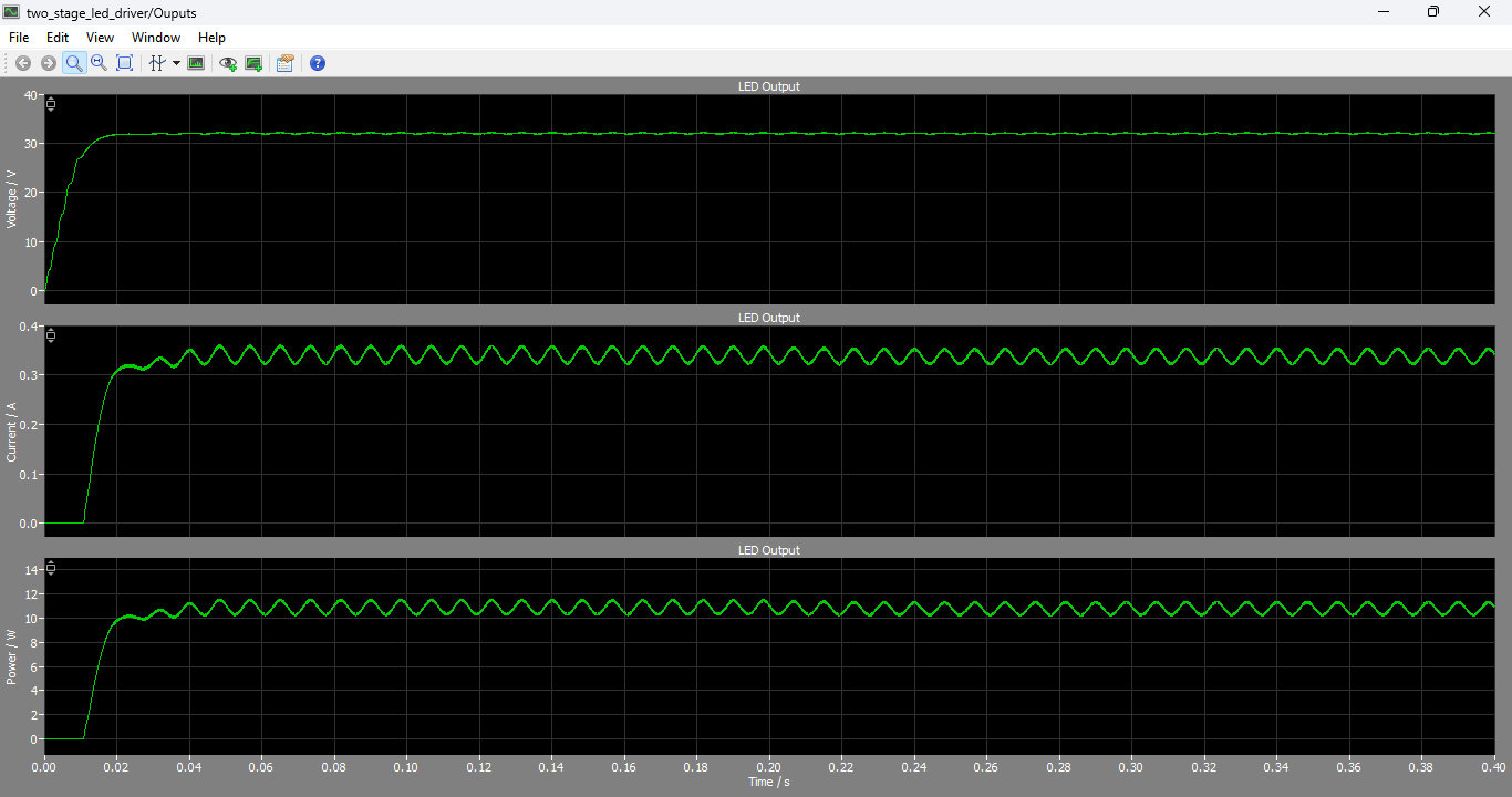
Figure 7: Simulated Flyback converter output characteristics showing the LED output voltage, output current, and output power.
You can download the Project files here: Download files now. (You must be logged in).
The output voltage rapidly reaches the desired reference value following the startup transient with only a small overshoot and negligible steady-state ripple. The fast settling time demonstrates the effectiveness of the voltage controller designed using the K-factor loop-shaping method. Stable voltage regulation ensures reliable operation of the LED load even under varying operating conditions.
The LED output current remains nearly constant throughout the simulation with only a small ripple component superimposed on the average value. Low current ripple is particularly important for LED lighting applications because it minimizes fluctuations in luminous intensity, reduces thermal stress within the semiconductor junctions, and contributes to improved device reliability and extended operational lifetime.
The output power waveform also reaches a stable value shortly after converter startup, indicating continuous and efficient energy transfer from the input source to the LED load. The absence of significant oscillations or power fluctuations confirms the stable dynamic performance of the complete two-stage converter. Furthermore, the Flyback topology provides galvanic isolation between the AC mains supply and the LED load, enhancing electrical safety while maintaining accurate output regulation.
Overall, the simulation results demonstrate that the proposed Flyback converter successfully achieves stable output voltage regulation, low current ripple, and consistent power delivery, validating its suitability for high-efficiency LED driver applications.
D. Overall Performance Discussion
Simulation results demonstrate that each stage of the proposed converter successfully performs its intended function. The Boost converter achieves excellent power factor correction while maintaining a regulated intermediate DC bus. Simultaneously, the Flyback converter provides isolated voltage regulation with low output ripple and stable steady-state performance.
Several advantages of the proposed design may therefore be summarized as follows:
- High input power factor approaching unity.
- Low total harmonic distortion.
- Stable intermediate DC-link voltage.
- Excellent LED output voltage regulation.
- Low output current ripple.
- Fast transient response.
- Electrical isolation between supply and load.
- Simple controller implementation using analytical design techniques.
- Suitability for residential, commercial, and industrial lighting systems.
The simulation results confirm that the proposed converter architecture provides an efficient and reliable solution for modern LED lighting applications.
VI. Conclusion
This paper presented the design, modeling, and simulation of a two-stage LED driver consisting of a Boost Power Factor Correction converter followed by an isolated Flyback DC–DC converter. The complete system was developed using the PLECS simulation platform and analyzed under steady-state operating conditions.
The Boost converter effectively corrected the input power factor by shaping the input current to follow the supply voltage while simultaneously regulating the intermediate DC-link voltage. The Flyback converter successfully provided galvanic isolation together with accurate voltage regulation for the LED load. Independent controller design using the analytical K-factor method resulted in stable converter operation, rapid transient response, and improved robustness.
Simulation results demonstrated low harmonic distortion, high power factor, excellent output voltage regulation, and low output current ripple. These characteristics indicate that the proposed converter is capable of satisfying the performance requirements of modern high-efficiency LED lighting systems.
The study further illustrates the usefulness of PLECS as an effective simulation environment for power electronic converter analysis, enabling controller verification and system optimization before hardware implementation.
VII. Future Work
Future investigations may extend this work in several directions. Hardware implementation of the proposed converter would allow experimental validation of the simulation results under practical operating conditions. Digital controller implementation using DSP or FPGA platforms may also be investigated to improve flexibility and computational performance.
Additional research may focus on adaptive control techniques capable of maintaining optimal performance under varying load conditions. Advanced soft-switching methods, synchronous rectification, and wide-bandgap semiconductor devices such as silicon carbide (SiC) and gallium nitride (GaN) transistors may further improve converter efficiency while reducing switching losses.
Integration of intelligent monitoring systems and Internet of Things (IoT) communication can also enable predictive maintenance and remote control of future smart lighting systems.
References
[1] S. Y. Hui, S. Y. R. Hui, and X. H. Tao, “A new generation of solid-state lighting,” IEEE Power Electronics Magazine, vol. 1, no. 2, pp. 22–31, 2014.
[2] N. Mohan, T. M. Undeland, and W. P. Robbins, Power Electronics: Converters, Applications, and Design, 3rd ed. Hoboken, NJ, USA: Wiley, 2003.
[3] IEEE Recommended Practice and Requirements for Harmonic Control in Electric Power Systems, IEEE Standard 519-2014, 2014.
[4] R. W. Erickson and D. Maksimović, Fundamentals of Power Electronics, 2nd ed. New York, NY, USA: Springer, 2001.
[5] R. Redl and N. O. Sokal, “A new family of single-stage isolated power-factor correctors,” IEEE Transactions on Power Electronics, vol. 13, no. 4, pp. 701–705, 1998.
[6] J. Sebastian, D. G. Lamar, M. Arias, and A. Rodriguez, “High-power-factor LED drivers,” IEEE Transactions on Industry Applications, vol. 50, no. 3, pp. 2085–2095, 2014.
[7] R. Ayyanar, “K-factor based compensator design for switched-mode power converters,” Arizona State University, Lecture Notes, 2016.
[8] Plexim GmbH, PLECS User Manual, Zurich, Switzerland, 2023.
[9] H. van der Broeck, G. Sauerländer, and M. Wendt, “Power driver topologies for LEDs,” IEEE Industry Applications Magazine, vol. 13, no. 4, pp. 31–38, 2007.
[10] L. Huber and M. M. Jovanović, “Design-oriented analysis of Boost PFC converters,” IEEE Transactions on Power Electronics, vol. 15, no. 3, pp. 468–479, 2000.
[11] R. Ridley, Loop Control for Switching Power Supplies. Colorado Springs, CO, USA: Ridley Engineering, 2011.
[12] B. Singh, B. N. Singh, A. Chandra, K. Al-Haddad, A. Pandey, and D. P. Kothari, “A review of power factor correction techniques,” IEEE Transactions on Industrial Electronics, vol. 50, no. 5, pp. 962–981, 2003.
[13] R. Ayyanar, “Loop shaping and K-factor design methodology for DC–DC converters,” Arizona State University, Technical Notes, 2015.
[14] C. K. Tse, Complex Behavior of Switching Power Converters. Boca Raton, FL, USA: CRC Press, 2003.
[15] D. Hart, Power Electronics. New York, NY, USA: McGraw-Hill, 2011.
[16] M. H. Rashid, Power Electronics Handbook, 4th ed. Oxford, U.K.: Butterworth-Heinemann, 2018.
[17] B. K. Bose, Modern Power Electronics and AC Drives. Upper Saddle River, NJ, USA: Prentice Hall, 2002.
[18] IEC 61000-3-2, Electromagnetic Compatibility (EMC)—Limits for Harmonic Current Emissions, International Electrotechnical Commission, 2018.
You can download the Project files here: Download files now. (You must be logged in).








Responses