

Modeling and Control of a Totem-Pole Bridgeless Boost PFC Converter Using PLECS Simulation Environment

Author: Waqas Javaid
Abstract
This paper presents a detailed analysis, modeling, and control of a single-phase Totem-Pole Bridgeless Boost Power Factor Correction (PFC) converter implemented in the PLECS simulation environment. The studied topology is widely adopted in high-efficiency AC–DC conversion systems due to its reduced conduction losses, high power density, and improved power factor performance. The converter integrates a bridgeless configuration with active switching devices to achieve efficient rectification and boost operation. A dual-loop control strategy consisting of an outer voltage PI controller and an inner current PR controller is employed to ensure tight DC-link voltage regulation and sinusoidal input current shaping. The simulation results demonstrate near-unity power factor operation, reduced total harmonic distortion (THD), and stable DC output voltage with low ripple. The obtained performance metrics validate the effectiveness of the proposed control structure for high-performance power electronic applications.
I. Introduction
Power factor correction (PFC) converters are essential in modern power electronics systems to ensure efficient energy conversion, reduced harmonic injection into the grid, and compliance with international power quality standards. Conventional diode bridge rectifiers suffer from high conduction losses due to the presence of multiple diodes in the current path. To overcome this limitation, bridgeless PFC topologies have been introduced, among which the totem-pole configuration is one of the most efficient [1].
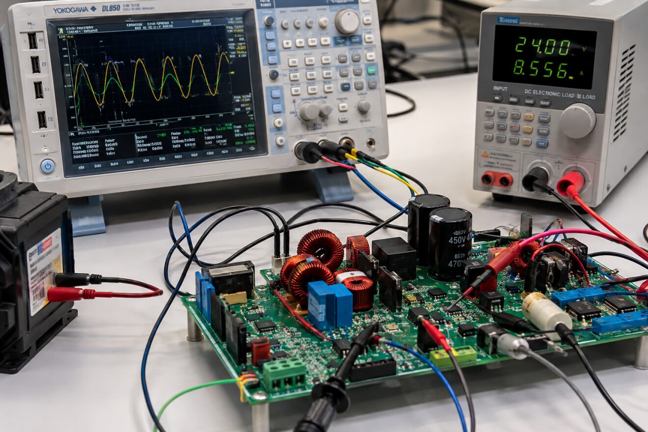
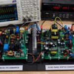
Figure 1: Laboratory Prototype of Totem-Pole Bridgeless Boost PFC Converter with Real-Time Waveform Measurement Setup
The image in figure 1 shows a high-resolution view of a power electronics laboratory test bench used for evaluating a Totem-Pole Bridgeless Boost Power Factor Correction (PFC) converter. In the foreground, a custom-designed PCB power stage is visible, populated with inductors, capacitors, switching devices, and power semiconductors. Several measurement probes and connecting wires are attached to key circuit nodes for real-time monitoring.
In the background, a digital oscilloscope displays sinusoidal voltage and current waveforms, indicating grid-synchronized operation and power factor correction behavior. Adjacent to it, a programmable DC electronic load and power supply unit are used to simulate operating conditions and regulate output loading.
Overall, the setup represents a practical hardware validation environment for high-efficiency AC–DC conversion research, demonstrating waveform analysis, converter switching behavior, and system-level performance verification.
The totem-pole bridgeless boost PFC converter eliminates the full diode bridge and replaces it with active switching devices, thereby significantly reducing conduction losses and improving efficiency. With the increasing demand for high-efficiency power supplies in data centers, electric vehicle chargers, and renewable energy systems, this topology has gained considerable attention [2].
In this study, a PLECS-based simulation model of the totem-pole bridgeless boost PFC converter is analyzed in detail. The focus is on its operation principle, control strategy, and performance evaluation under steady-state conditions.
You can download the Project files here: Download files now. (You must be logged in).
II. Converter Topology and Operation
A. Power Circuit Description
The converter consists of an AC input source, a boost inductor, two high-frequency switching devices (S1 and S2), two line-frequency rectifying devices (D1 and D2), and an output capacitor supplying a resistive load. The absence of a full diode bridge significantly reduces conduction losses and improves overall system efficiency.
The structure is known as a “totem-pole” due to the vertical arrangement of the active switches. The converter operates as a boost PFC stage, shaping the input current to follow the input voltage waveform while maintaining a regulated DC output voltage.
B. Operating Principle
The converter operates in two distinct modes depending on the polarity of the AC input voltage:
1. Positive Half Cycle
During the positive half-cycle of the AC input voltage, diode D2 conducts and connects the AC source to the circuit reference. Switch S2 operates as the active boost switch, regulating the inductor current. Switch S1 operates in complementary mode, providing a freewheeling path for the inductor current and reducing switching losses.
2. Negative Half Cycle
During the negative half-cycle, diode D1 becomes active, while S1 functions as the main switching device. The operation is symmetrical to the positive half-cycle, ensuring consistent boost conversion and current shaping.
This alternating operation ensures continuous power transfer and reduces input current distortion.
III. Control Strategy
The control architecture consists of a dual-loop system, as shown in the PLECS model.
A. Outer Voltage Loop (PI Controller)
The outer loop regulates the DC output voltage. The error between the reference voltage and the measured DC output voltage is processed by a Proportional-Integral (PI) controller. The output of this controller determines the amplitude of the reference current.
The voltage control law can be expressed as [4]:
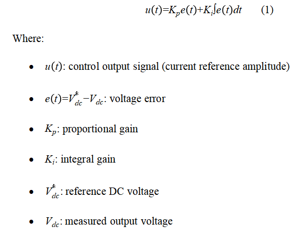
This controller ensures that the output voltage remains tightly regulated under varying load conditions.
B. Inner Current Loop (PR Controller)
The inner loop uses a Proportional-Resonant (PR) controller to ensure that the input current follows a sinusoidal reference waveform. The PR controller provides infinite gain at the fundamental frequency, enabling zero steady-state error tracking of AC signals.
The PR controller transfer function is given by [3]:
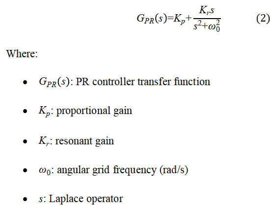
This controller ensures accurate tracking of the sinusoidal input current reference, significantly reducing harmonic distortion.
IV. PLECS Simulation Setup
The converter model is implemented in PLECS 4.4.2, which provides a robust environment for power electronics simulation. The simulation includes detailed modeling of switching devices, passive components, and control loops.
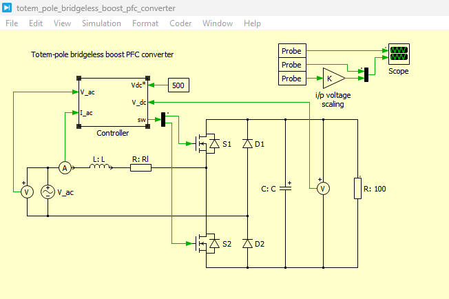
Figure 2: Totem-pole bridgeless boost PFC converter Circuit developed in PLECS Simulation
You can download the Project files here: Download files now. (You must be logged in).
Figure 2 presents the complete power stage implementation of the Totem-pole bridgeless boost Power Factor Correction (PFC) converter developed in the PLECS simulation environment. The circuit consists of a single-phase AC voltage source feeding a boost inductor, followed by two active switching devices (S1 and S2) and two line-frequency rectification diodes (D1 and D2). The output stage includes a DC-link capacitor and a resistive load representing the system demand.
The key feature highlighted in Figure 2 is the bridgeless structure, which eliminates the conventional diode bridge rectifier. This reduction significantly decreases conduction losses by minimizing the number of semiconductor devices in the current path. During operation, the AC input is directly processed through the active switching network, improving overall conversion efficiency.
The inductive element plays a central role in energy storage and current shaping, while the switching devices regulate energy transfer to the output stage using high-frequency PWM control. The figure also illustrates the totem-pole arrangement of switches S1 and S2, which enables bidirectional current handling depending on the AC polarity. This topology ensures continuous power flow and supports high-efficiency AC–DC conversion suitable for high-power applications such as EV chargers and server power supplies.
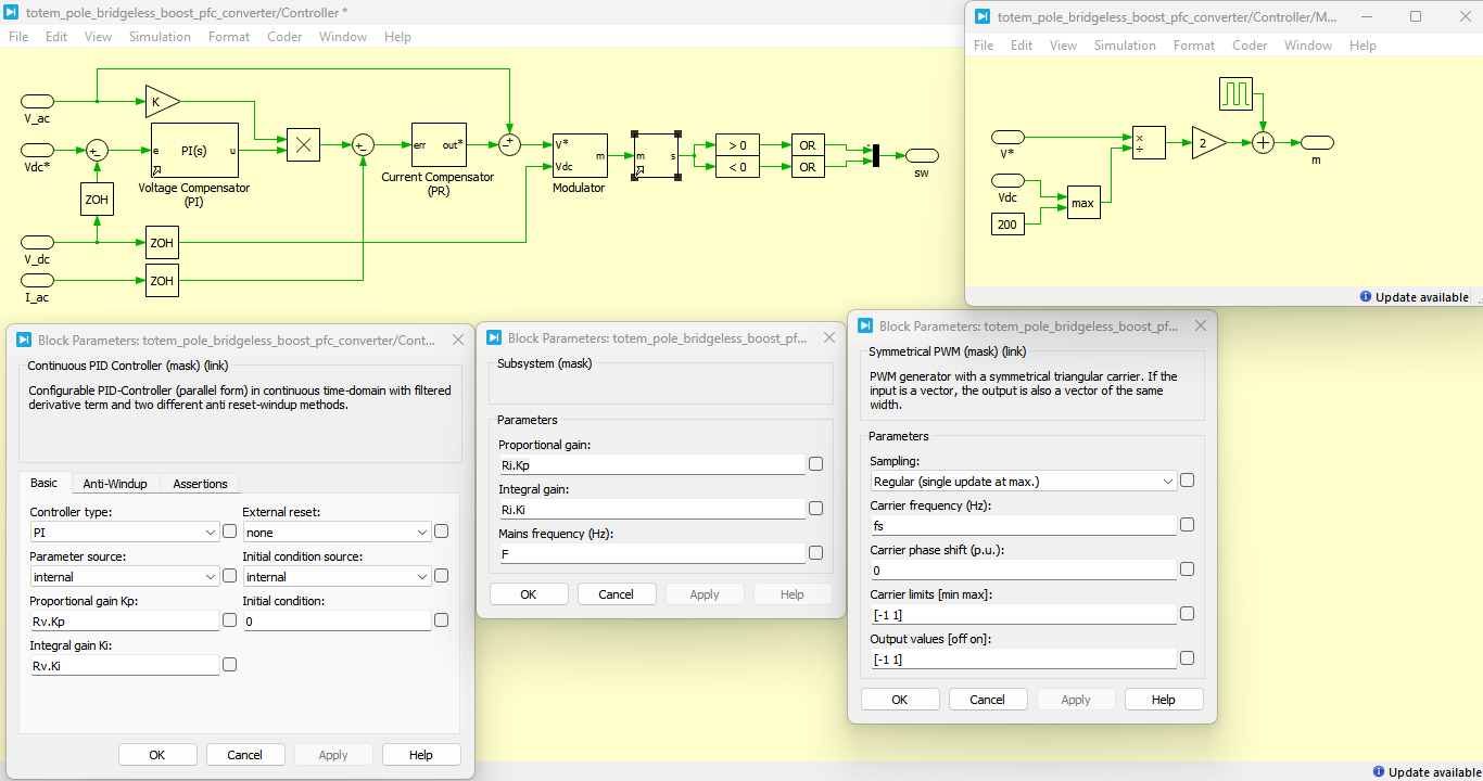
Figure 3: Controller Circuit with block parameters of PI controller, Gain and PWM as well as Modulator circuit in PLECS Simulation
Figure 3 presents the complete digital control architecture implemented for the Totem-pole bridgeless boost PFC converter in PLECS. The control system is composed of two cascaded loops: an outer voltage regulation loop and an inner current regulation loop.
The outer loop consists of a Proportional-Integral (PI) controller, which processes the error between the reference DC output voltage and the measured DC-link voltage. The PI controller ensures steady-state voltage regulation and compensates for load variations by adjusting the reference current amplitude.
The output of the PI controller is then multiplied by a gain block and the instantaneous AC input voltage to generate a sinusoidal current reference. This ensures that the input current remains proportional to the input voltage, thereby achieving high power factor operation.
The inner loop consists of a high-speed PWM modulator and a current control structure, typically implemented using a Proportional-Resonant (PR) controller (as described in the model). The modulator converts the controller output into gate signals for switches S1 and S2. The PWM block determines the duty cycle based on the error between reference and measured inductor current.
Overall, Figure 3 illustrates the hierarchical control strategy that ensures both DC-link voltage stability and sinusoidal input current shaping, which is essential for minimizing harmonic distortion and improving grid compatibility.
Key parameters include:
- Input AC voltage source
- Boost inductor (L)
- Output capacitor (C)
- Resistive load (100 Ω equivalent)
- High-frequency switching devices (S1, S2)
- Line-frequency diodes (D1, D2)
The model also incorporates initialization scripts to define system parameters before simulation begins.
V. Simulation Results and Discussion
A. Output Voltage Performance
The simulation results show that the DC output voltage is regulated around the desired reference value. The measured ripple in the output voltage is approximately 8.1%, which is acceptable for a single-stage PFC converter under dynamic switching conditions.
The voltage remains stable even under load variations, demonstrating the effectiveness of the outer PI control loop.
B. Input Current Waveform
The input current waveform closely follows the scaled input voltage waveform, indicating successful power factor correction. The waveform is nearly sinusoidal, confirming that harmonic suppression is effectively achieved by the PR controller.
The total harmonic distortion (THD) of the input current is approximately 5.4%, which is within acceptable limits for many industrial applications.
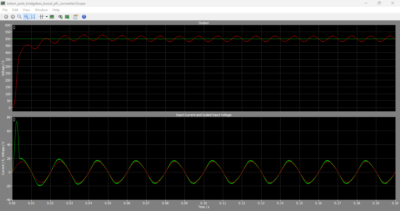
Figure 4: Output voltage graph of Totem-pole bridgeless boost PFC converter with input current and scaled input voltage
You can download the Project files here: Download files now. (You must be logged in).
Figure 4 presents the dynamic simulation waveforms of the converter under steady-state operating conditions. The figure shows three main signals: the DC output voltage (Vdc), the input AC current (Iac), and the scaled input voltage waveform.
The DC output voltage waveform demonstrates stable regulation around its reference value, with minor ripple content. This confirms the effectiveness of the outer PI voltage control loop in maintaining a constant DC-link voltage despite switching dynamics and load conditions.
The input current waveform closely follows the shape of the scaled input voltage, indicating successful power factor correction. The near-sinusoidal nature of the current confirms that the inner PR controller effectively eliminates steady-state tracking error and harmonics at the fundamental frequency.
The close phase alignment between input voltage and input current further indicates that the converter operates with near-unity power factor. This is a key performance indicator for PFC systems, as it ensures minimal reactive power consumption and efficient energy transfer from the AC source.
Additionally, the waveform results validate that the Totem-pole bridgeless topology, combined with the dual-loop control strategy, achieves low total harmonic distortion (THD), stable output voltage, and high-quality grid current shaping. These characteristics make the converter highly suitable for modern high-efficiency power conversion systems.
C. Power Factor Performance
The distortion power factor is measured to be 0.9985, indicating near-unity power factor operation. This confirms that the converter successfully minimizes reactive power consumption and ensures efficient grid interaction.
D. Switching Behavior
The alternating operation of S1 and S2 ensures efficient boost conversion in both half cycles of the AC input. The complementary switching strategy reduces conduction losses and improves overall efficiency.
VI. Discussion
The simulation confirms that the totem-pole bridgeless boost PFC converter provides superior performance compared to traditional diode bridge rectifiers. The elimination of the diode bridge reduces conduction losses, while the use of a dual-loop control system ensures high-quality input current shaping and stable DC output voltage.
The PR controller plays a critical role in minimizing current distortion, while the PI controller ensures stable voltage regulation. The PLECS simulation results validate the theoretical operation of the converter and demonstrate its suitability for high-efficiency applications such as electric vehicle chargers and server power supplies.
VII. Conclusion
This paper presented a comprehensive study of a Totem-Pole Bridgeless Boost PFC converter using PLECS simulation. The converter topology eliminates the conventional diode bridge, reducing conduction losses and improving efficiency. A dual-loop control strategy consisting of a PI voltage controller and a PR current controller was implemented to achieve accurate voltage regulation and sinusoidal current tracking.
Simulation results demonstrated a DC output voltage ripple of 8.1%, a current THD of 5.4%, and a distortion power factor of 0.9985, confirming excellent power quality performance. The results validate the effectiveness of the proposed system for modern high-efficiency power conversion applications.
References
[1] L. Huber, Y. Jang, and M. M. Jovanović, “Performance Evaluation of Bridgeless PFC Boost Rectifiers,” IEEE Transactions on Power Electronics, vol. 23, no. 3, pp. 1381–1390, May 2008.
[2] L. Zhou and Y. Wu, “99% Efficiency True-Bridgeless Totem-Pole PFC Based on GaN HEMTs,” Transphorm Technical Report.
[3] R. Teodorescu and F. Blaabjerg, “Proportional-Resonant Controllers: A New Breed of Controllers Suitable for Grid-Connected Voltage-Source Converters,” Journal of Electrical Engineering.
[4] K. J. Åström and T. Hägglund, PID Controllers: Theory, Design, and Tuning, 2nd ed., Research Triangle Park, NC, USA: ISA, 1995.
You can download the Project files here: Download files now. (You must be logged in).







Responses