

Three-Output Flyback Converter with PI-Based Analog Control Using PLECS Simulation

Author: Waqas Javaid
Abstract
This paper presents the modeling, simulation, and performance evaluation of a three-output flyback DC–DC converter implemented using the PLECS simulation environment. The converter is designed to generate three regulated output voltages of +15 V, +5 V, and −15 V from a single DC input source using a multi-winding transformer. A closed-loop analog control scheme based on a proportional–integral (PI) controller is applied to regulate the +5 V output, while the remaining outputs are cross-regulated through transformer coupling. Pulse-width modulation (PWM) is used to control the switching behavior of the MOSFET switch. The system is analyzed under steady-state and dynamic load variation conditions, including a step change in the load resistance at the +5 V output. Simulation results demonstrate the effectiveness of the PI controller in maintaining voltage regulation within specified tolerance limits under varying load conditions. The study highlights the importance of control design in multi-output isolated converters and validates the robustness of analog PI control in flyback converter applications.
1. Introduction
DC–DC converters play a crucial role in modern power electronics systems, particularly in applications requiring isolated voltage levels and multiple regulated outputs such as embedded systems, industrial power supplies, and communication circuits. Among isolated converter topologies, the flyback converter is widely used due to its simplicity, low component count, and ability to provide multiple output voltages using a single transformer [1].
The flyback converter operates on the principle of energy storage in the transformer magnetizing inductance during the ON state of the switch and energy transfer to secondary windings during the OFF state. This makes it suitable for low-to-medium power applications. However, in multi-output configurations, cross-regulation becomes a significant challenge due to load dependency across secondary windings [2].
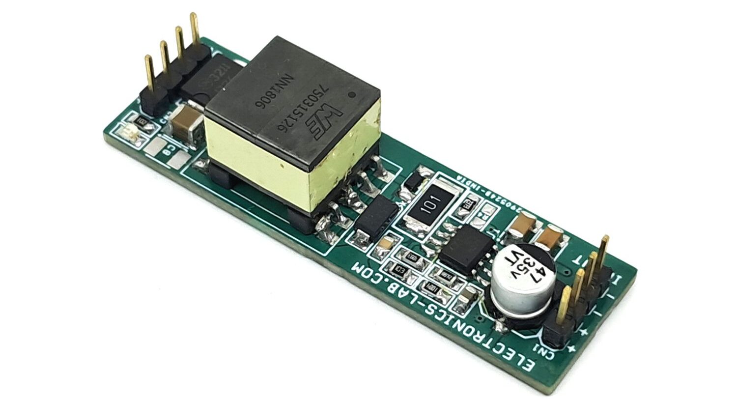
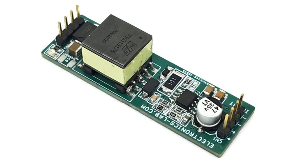
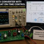
Figure 1: Isolated Flyback Converter Hardware Board for Testing Real-Time Power Supply Applications
Figure 1 presents the practical hardware implementation of an isolated flyback converter designed for real-time testing in power supply applications. This hardware setup is used to validate simulation results under actual operating conditions [3].
The converter consists of a high-frequency switching MOSFET, a flyback transformer with multiple secondary windings, rectifier diodes, filtering capacitors, and a control interface. The isolation provided by the transformer ensures electrical safety between the input and output stages while enabling multiple output voltages [4].
In practical operation, the input DC supply is converted into high-frequency switching pulses using the MOSFET. These pulses are applied to the transformer primary winding, where energy is stored during the ON state and transferred to secondary windings during the OFF state. Each secondary winding generates a regulated output voltage such as +15 V, +5 V, and −15 V.
The hardware board also includes measurement points and feedback sensing circuits to monitor output voltages and switching behavior [5]. This allows researchers to observe real-time performance, efficiency, switching stress, and thermal behavior of components.
Overall, Figure 1 demonstrates the experimental validation platform for flyback converter studies, bridging the gap between theoretical modeling and real-world power electronics applications.
To address voltage regulation challenges, feedback-based control systems are commonly employed. In this work, a proportional–integral (PI) controller is used to regulate the 5 V output, while the remaining outputs (+15 V and −15 V) are indirectly regulated through transformer coupling [6]. The PI controller adjusts the duty cycle of a PWM signal driving the MOSFET switch, ensuring stable output voltage under dynamic load variations [7].
The system is modeled and simulated using the PLECS environment developed by Plexim GmbH, which provides a powerful platform for power electronics simulation and control system design.
You can download the Project files here: Download files now. (You must be logged in).
2. System Description
2.1 Flyback Converter Topology
The studied system consists of a three-output flyback converter with one primary winding and three secondary windings. The input DC voltage is applied to the primary side of a transformer, while secondary windings generate:
- +15 V output
- +5 V regulated output
- −15 V output
The energy transfer mechanism follows two stages:
- Switch ON State: Energy is stored in the transformer magnetizing inductance.
- Switch OFF State: Stored energy is transferred to secondary outputs.
This operation enables electrical isolation and multiple voltage generation using a single magnetic core [8].
Unlike ideal theoretical models, practical implementations include parasitic elements such as leakage inductance, winding resistance, and switching losses. However, the present PLECS model assumes an ideal transformer to focus on control performance analysis.
2.2 Load Configuration and Disturbance
A dynamic load condition is introduced at the +5 V output. A resistive load step is applied midway through the simulation by reducing the load resistance to test the robustness of the controller. This disturbance simulates real-world scenarios where digital circuits or embedded systems may experience sudden current demand changes.
The converter is expected to maintain output voltage regulation within:
- ±0.5 V tolerance for low-voltage output
- ±1 V tolerance for higher voltage outputs
3. Control System Design
3.1 Voltage Regulation Strategy
Voltage regulation is performed only on the +5 V output using a closed-loop feedback system. The measured output voltage is compared with a reference voltage (5 V), and the resulting error is processed by a PI controller.
This control signal is then used to adjust the modulation index of the PWM generator, which ultimately controls the MOSFET switching behavior.
3.2 PI Controller Formulation
The PI controller is mathematically expressed as [1][2]:
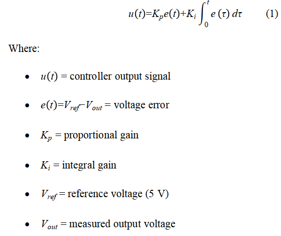
The proportional term provides immediate response to error, while the integral term eliminates steady-state error by accumulating past deviations.
3.3 PWM Modulation Strategy
The PI controller output is converted into a duty cycle signal for PWM switching. The relationship can be expressed as [3]:
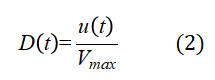
Where:
- D(t) = PWM duty cycle
- u(t) = PI controller output
- Vmax = maximum control signal scaling factor
The duty cycle determines the ON-time of the MOSFET switch, thereby controlling energy transfer in the transformer.
4. Simulation Setup
The converter is modeled and simulated in PLECS using ideal components. The simulation includes:
- DC input source
- Three-winding transformer
- MOSFET switching device
- PWM modulator
- PI control loop
- Resistive loads for each output
The simulation is executed with a load disturbance introduced at half the simulation time. The system response is analyzed in terms of:
- Output voltage stability
- Transient response
- Cross-regulation behavior
- Control effectiveness
5. Results and Discussion
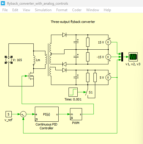
Figure 2: Three output flyback converter model in PLECS Simulation
You can download the Project files here: Download files now. (You must be logged in).
Figure 2 illustrates the PLECS-based simulation model of the three-output flyback converter. This model represents an idealized version of the hardware system and is used to analyze electrical behavior and control performance under controlled conditions.
The model includes a DC input source, a MOSFET switching device, a three-winding transformer, and three separate output rectifier-filter networks producing +15 V, +5 V, and −15 V outputs. Each output is connected to independent resistive loads, allowing the study of load variation effects.
A key feature of this simulation model is that only the +5 V output is regulated using a closed-loop control system, while the other two outputs depend on transformer coupling. This creates a realistic multi-output scenario where cross-regulation effects can be observed.
The PLECS environment developed by Plexim GmbH enables fast switching simulation, accurate power electronics modeling, and integrated control design. The model allows observation of waveforms such as output voltage stability, inductor current behavior, and transient response under load changes [9].
Thus, Figure 2 serves as the core simulation platform for analyzing converter performance and verifying control strategies.
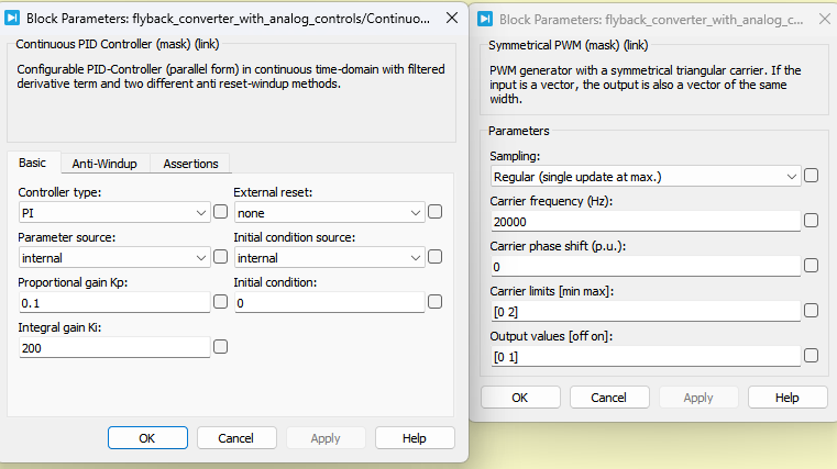
Figure 3: Block Parameters of Continuous PID Controller and PWM generator
Figure 3 shows the control system implementation, consisting of a continuous PID (PI-based) controller and a PWM generator block used for switching control of the MOSFET.
The PID controller receives the error signal, which is the difference between the reference voltage (5 V) and the measured output voltage. This error is processed through proportional and integral actions to produce a control signal that minimizes voltage deviation.
The proportional component provides immediate correction based on current error, while the integral component eliminates steady-state error by accumulating past deviations. This ensures accurate voltage regulation even under varying load conditions.
The output of the PID controller is fed into the PWM generator, which converts the analog control signal into a high-frequency switching pattern. The duty cycle of the PWM signal is adjusted dynamically based on controller output, controlling the energy transferred through the transformer.
Key parameters in this block include:
- Proportional gain (Kp)
- Integral gain (Ki)
- PWM switching frequency
- Duty cycle limits (saturation bounds)
This control structure ensures stable operation of the flyback converter by maintaining consistent output voltage and minimizing oscillations.
5.1 Steady-State Performance
Under steady-state conditions, all three outputs stabilize at their nominal values:
- +15 V output remains stable with minimal ripple
- −15 V output maintains symmetric regulation
- +5 V output achieves precise regulation due to closed-loop control
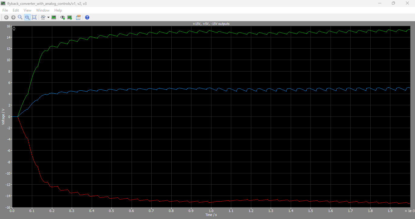
Figure 4: Output voltages of flyback converter with different levels +15V, +5V, -15V
You can download the Project files here: Download files now. (You must be logged in).
Figure 4 presents the simulation results of output voltage waveforms for all three outputs of the flyback converter: +15 V, +5 V, and −15 V.
The waveforms demonstrate that the converter successfully generates three stable DC voltage levels from a single input source. The +5 V output is tightly regulated using the PI control loop, maintaining minimal ripple and high stability even during load disturbances.
The +15 V and −15 V outputs are derived from transformer secondary windings and are indirectly regulated. Although not directly controlled, they maintain relatively stable voltage levels due to proper transformer design and energy distribution across windings.
During simulation, a load disturbance is introduced at the +5 V output. This causes a temporary voltage drop; however, the PI controller quickly responds by adjusting the PWM duty cycle, restoring the voltage to its reference value. The other outputs show minor deviations due to cross-regulation effects but remain within acceptable tolerance limits.
Overall, Figure 4 confirms the effectiveness of closed-loop control in maintaining voltage stability and demonstrates the capability of multi-output flyback converters to deliver reliable power under dynamic conditions.
The PID controller effectively eliminates steady-state error, ensuring the regulated output remains close to the reference voltage.
5.2 Dynamic Response Under Load Disturbance
When the load resistance at the +5 V output is suddenly reduced, a sharp increase in load current occurs. This leads to an initial voltage drop. However, the PI controller reacts by increasing the duty cycle of the PWM signal, restoring the output voltage to its reference value.
Key observations include:
- Fast transient response of the control loop
- Minimal overshoot in output voltage
- Stable recovery within a short settling time
This demonstrates the robustness of PI control in handling sudden load variations.
5.3 Cross-Regulation Behavior
Since only the +5 V output is directly regulated, the +15 V and −15 V outputs depend on transformer coupling. During load disturbances:
- Slight voltage deviation is observed in unregulated outputs
- The deviations remain within acceptable tolerance limits
- Cross-regulation is inherently stable due to transformer design
However, under extreme load conditions, cross-regulation deteriorates, indicating the limitation of single-loop control in multi-output systems.
5.4 Stability Analysis
The system remains stable under all simulated conditions. The PI controller ensures:
- Zero steady-state error for controlled output
- Dampened oscillations during transient conditions
- Stable duty cycle variation without saturation
The results confirm that analog PI control is sufficient for low-complexity multi-output flyback systems.
6. Conclusion
This paper presented a detailed analysis of a three-output flyback converter using PLECS simulation with analog PI-based control. The system successfully generates +15 V, +5 V, and −15 V outputs from a single DC source. Closed-loop regulation of the +5 V output ensures stable operation under varying load conditions.
The PI controller demonstrated strong performance in maintaining voltage stability, reducing transient errors, and restoring output voltage after load disturbances. However, cross-regulation limitations were observed in the unregulated outputs, which is a known challenge in multi-output flyback topologies.
Future improvements may include:
- Multi-loop control strategies
- Digital control implementation using microcontrollers
- Synchronous rectification for improved efficiency
- Inclusion of non-ideal parasitic effects for real-world accuracy
Overall, the study confirms that PLECS is a powerful tool for analyzing and designing power electronic converters with control systems.
References
[1] N. Mohan, T. M. Undeland, and W. P. Robbins, Power Electronics: Converters, Applications and Design, Wiley.
[2] R. W. Erickson and D. Maksimović, Fundamentals of Power Electronics, Springer.
[3] Marian K. Kazimierczuk, Pulse-Width Modulated DC–DC Power Converters, 2nd ed., Wiley, 2015.
[4] Plexim GmbH, “PLECS User Manual and Demo Models Documentation,” 2023.
[5] M. H. Rashid, Power Electronics: Circuits, Devices and Applications, Pearson.
[6] B. K. Bose, Modern Power Electronics and AC Drives, Prentice Hall.
[7] J. G. Kassakian, M. F. Schlecht, and G. C. Verghese, Principles of Power Electronics, Addison-Wesley.
[8] A. Prodic and D. Maksimovic, “Digital PI Control of DC–DC Converters,” IEEE Transactions on Power Electronics.
[9] S. Cuk, “Switching DC-to-DC Converters,” IEEE Industry Applications Society.
You can download the Project files here: Download files now. (You must be logged in).







Responses