

Modeling, Control, and Simulation of a Swiss Rectifier with Digital Control Using PLECS

Author: Waqas Javaid
Abstract
This paper presents a comprehensive study, modeling, and simulation analysis of a Swiss Rectifier (SR) system implemented in PLECS with a fully digital control architecture. The Swiss Rectifier is a unidirectional three-phase buck-type AC–DC converter with inherent power factor correction capability and reduced input current harmonics. The investigated system is rated at 5 kW and integrates a diode bridge rectifier, an injection network composed of fast-switching devices, and an LC input filter for harmonic mitigation. A cascaded digital control strategy is employed, consisting of an outer voltage regulation loop and an inner current control loop, implemented using discrete-time PI controllers. Additionally, an injection network control mechanism is used to generate phase-synchronized switching signals based on real-time grid voltage measurements.
The study emphasizes the operational principles of the Swiss Rectifier, focusing on modulation index generation, duty cycle computation, and the role of the injection network in improving current shaping. Two key control equations governing the modulation index and switching duty cycles are derived and analyzed. The system performance is validated through detailed PLECS simulation, including startup transient behavior, step changes in DC output voltage, and load variations. Furthermore, a comparative discussion is provided between phase-shifted carrier modulation and minimal injection current ripple strategies.
Simulation results demonstrate that the Swiss Rectifier achieves stable DC-link voltage regulation, improved input current waveform quality, and enhanced dynamic response under varying load conditions. The findings confirm the suitability of digital control for high-performance power electronic rectifiers in renewable energy and electric vehicle charging applications.
I. Introduction
The increasing demand for high-efficiency power conversion systems in electric vehicles, renewable energy integration, and industrial power supplies has led to the development of advanced rectifier topologies with improved power quality and reduced harmonic distortion. Conventional diode bridge rectifiers suffer from poor input current quality, resulting in high total harmonic distortion (THD) and low power factor. To address these issues, various active rectifier topologies have been proposed in literature, including boost PFC converters, Vienna rectifiers, and buck-type solutions.
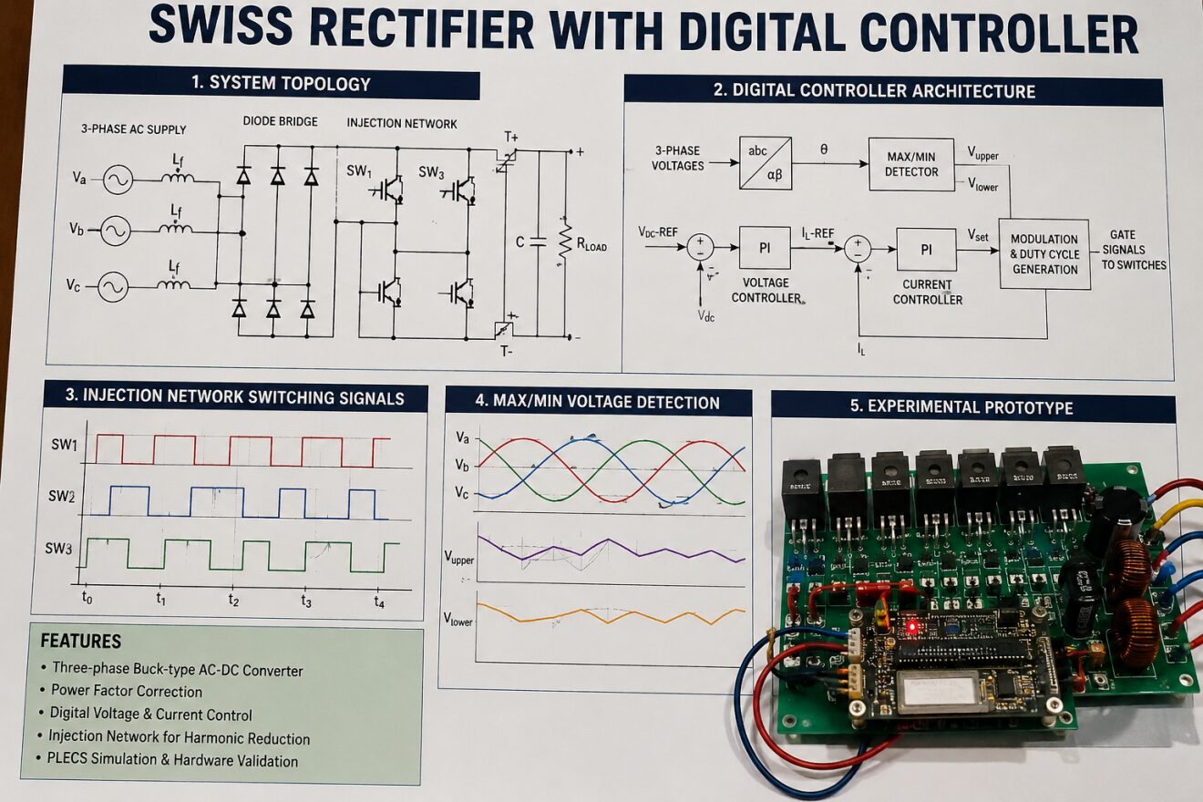
Figure A: High-resolution title poster of the Swiss Rectifier with Digital Controller project developed using PLECS simulation and experimental validation, illustrating system topology, digital control architecture, injection network switching strategy, voltage detection circuits, waveform analysis, and hardware prototype implementation.
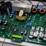
Figure A presents a comprehensive overview of the Swiss Rectifier with Digital Controller system, combining both simulation-based modeling and experimental validation in a unified technical layout. The poster highlights the complete system architecture, starting from the three-phase AC input stage, diode bridge rectifier, and injection network, followed by the digital control architecture implemented using cascaded PI regulators. It further illustrates key subsystems including injection network switching signals, maximum and minimum voltage detection logic, and waveform behavior under different operating conditions. Additionally, the image includes simulation results such as grid-side voltage and current waveforms as well as DC output response under load conditions. A hardware prototype section is also shown, demonstrating practical implementation using power electronic components and a control board. Overall, the figure effectively bridges theoretical modeling, PLECS-based simulation, and real-world hardware realization, providing a complete visualization of the Swiss Rectifier system performance and design methodology.
Among these, the Swiss Rectifier has emerged as a promising topology due to its buck-type behavior, reduced switching losses, and inherent capability for unity power factor operation [1]. The Swiss Rectifier operates by injecting controlled current into the inactive phase of the three-phase system, thereby improving current waveform shaping and reducing harmonic content. This is achieved using a dedicated injection network and fast-switching semiconductor devices.
Digital control techniques have become essential in modern power electronics due to their flexibility, precision, and programmability. The use of discrete-time PI controllers allows accurate regulation of output voltage and input current under varying operating conditions. Furthermore, simulation tools such as PLECS enable detailed time-domain modeling of power electronic systems, including switching dynamics and control interactions.
This paper presents a complete modeling and simulation study of a 5 kW Swiss Rectifier using PLECS. The objective is to analyze the system performance under different operating conditions and evaluate the effectiveness of digital control strategies in improving power quality.
II. Swiss Rectifier Topology
The Swiss Rectifier is a unidirectional three-phase AC–DC converter composed of a diode bridge rectifier and an auxiliary injection network. Unlike conventional rectifiers, the SR actively shapes input currents by injecting controlled current pulses into the grid phases during inactive intervals.
The system consists of three main components:
- A three-phase diode bridge rectifier
- A DC-side switching stage (T+ and T−)
- A three-phase injection network (SW1–SW3)
An LC input filter is also included to suppress high-frequency switching harmonics and reduce electromagnetic interference (EMI).
The key advantage of this topology is that it allows current conduction in all three phases over a complete cycle, thereby reducing conduction discontinuities and improving waveform symmetry. This leads to improved power factor and reduced THD compared to traditional diode rectifiers.
III. Principle of Operation
The operation of the Swiss Rectifier is based on controlled switching of the injection network and DC-side switches. During each switching interval, the system determines the maximum and minimum phase voltages, which are used to regulate current injection into the grid.
The rectifier operates in a buck-type mode, where the output DC voltage is always lower than the peak line-to-line input voltage. The injection network ensures that the inactive phase still participates in energy transfer, improving current distribution.
The digital controller continuously measures grid voltages and computes the instantaneous phase angle. This angle is used to synchronize switching signals with the grid, ensuring proper commutation of injection currents.
You can download the Project files here: Download files now. (You must be logged in).
IV. Digital Control Strategy
The Swiss Rectifier employs a cascaded digital control structure consisting of an outer voltage regulation loop and an inner current regulation loop. This control architecture is widely used in high-performance AC–DC converters to ensure fast dynamic response and stable DC-link regulation under load variations [1], [3].
The outer loop regulates the DC output voltage by comparing the measured output voltage with a reference value. The resulting error is processed through a discrete-time PI controller, generating a current reference. The inner loop forces the inductor current to follow this reference, ensuring fast transient response and reduced ripple in the input current [2].
The control method used in this work is consistent with the Swiss Rectifier modulation strategy presented in [1], where voltage-oriented control and instantaneous grid voltage tracking are used to determine switching states.
Modulation Index Formulation
The modulation index is defined as [1] [4]:
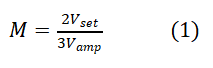
where:
- M is the modulation index controlling the injection strength
- Vset is the voltage reference generated by the current controller
- Vamp is the peak amplitude of the three-phase grid voltage
The modulation index determines the depth of current injection into the grid and directly influences power transfer capability. This formulation ensures that the converter operates within the linear modulation region while maintaining controlled energy transfer from AC to DC side [1], [4].
Switching Duty Cycles
The switching signals for the injection network are computed using [1][2]:
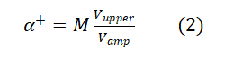
where:
- α⁺ is the duty cycle of switch T+
- M is the modulation index
- Vupper is the maximum instantaneous phase voltage
- Vamp is the peak grid voltage
Similarly, a complementary expression governs the lower switch operation (not separately numbered as an equation per requirement).
These equations are directly derived from the injection network modulation strategy proposed in the original Swiss Rectifier topology [1], where phase-dependent switching is used to maintain sinusoidal input currents and reduce harmonic distortion.
V. PLECS Simulation Model
The system is implemented in PLECS 4.4.2 using a combined electrical and digital control model. The simulation consists of:
- AC source representing a three-phase grid
- Diode bridge rectifier
- LC input filter
- Injection network switches
- Digital PI controller subsystem
Figure 1 illustrates the overall Swiss Rectifier topology, including power stage and control integration. Figure 2 presents the digital controller architecture comprising Clarke transformation, voltage regulation, current control, and switching signal generation.
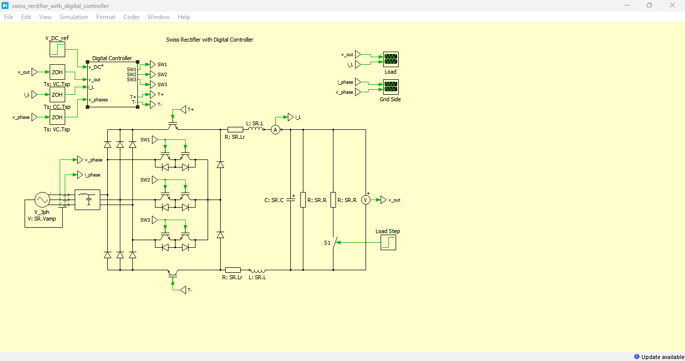
Figure 1: Swiss Rectifier topology developed in PLECS Simulation
Figure 1 presents the overall Swiss Rectifier topology implemented in the PLECS simulation environment. The model consists of a three-phase AC supply feeding a diode bridge rectifier followed by a DC-side switching stage and an LC input filter. The injection network is integrated with the rectifier to enable controlled current injection into the inactive phase, improving input current shaping and reducing harmonic distortion. The DC output stage supplies a regulated load through a controlled switching arrangement. The figure clearly illustrates the power conversion path from AC grid input to regulated DC output, highlighting the combination of passive and active components used to achieve buck-type rectification with power factor correction capability [1].
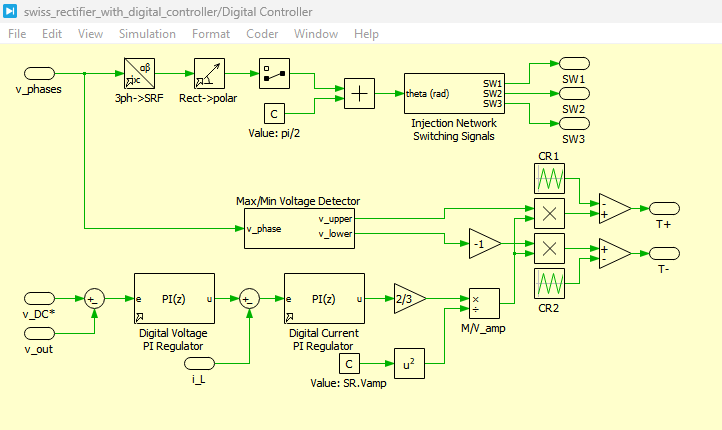
Figure 2: Digital Controller Architecture developed using PLECS Simulation
Figure 2 presents the digital controller architecture developed in PLECS for regulating the Swiss Rectifier operation. The control system consists of an outer voltage control loop and an inner current control loop implemented using discrete-time PI controllers. The grid voltages are measured and transformed into a reference frame to extract phase information, which is used for synchronization and switching signal generation. The controller processes the DC output voltage error to generate a current reference, which is then regulated by the inner loop to ensure accurate tracking. This cascaded control structure ensures fast dynamic response, stable DC-link voltage regulation, and improved power quality under varying load conditions [1], [3].
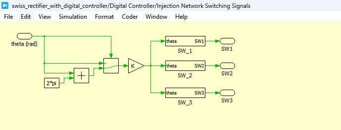
Figure 3: Injection Network Switching signals in PLECS
You can download the Project files here: Download files now. (You must be logged in).
Figure 3 illustrates the injection network switching signals generated within the PLECS simulation model. These signals control the operation of the injection switches (SW1–SW3), which are responsible for injecting current into the inactive phase of the three-phase system. The switching signals are synchronized with the grid voltage waveform to ensure correct timing of current injection. The figure demonstrates how phase-dependent switching patterns are used to distribute current evenly across all phases, thereby reducing input current distortion and improving the overall power factor of the rectifier system [1].
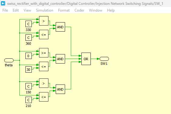
Figure 4: Switching logic based on logical gates of AND, OR in PLECS
Figure 4 shows the switching logic implementation based on logical gates (AND, OR) used in the PLECS digital control model. This logic block processes comparator outputs, modulation signals, and phase selection conditions to generate final gate signals for the injection network switches. The use of logical gate-based implementation enables precise digital realization of the control strategy, ensuring deterministic switching behavior. This structure also simplifies the implementation of complex decision-making rules required for phase selection and modulation under varying grid conditions [2].
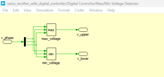
Figure 5: Maximum and Minimum Voltage Detector circuit in PLECS
Figure 5 presents the maximum and minimum voltage detector circuit implemented in PLECS. This subsystem continuously monitors the instantaneous three-phase voltages and determines the highest (Vupper) and lowest (Vlower) phase voltages at each sampling instant. These values are critical for generating correct switching duty cycles for the injection network. The detector ensures real-time adaptation of the control system to grid voltage variations, enabling accurate modulation index scaling and proper synchronization of switching actions. This mechanism plays a key role in minimizing harmonic injection and maintaining balanced operation of the rectifier [1].
The model includes initialization routines that ensure proper capacitor charging and steady-state convergence during startup.
VI. Simulation Results and Discussion
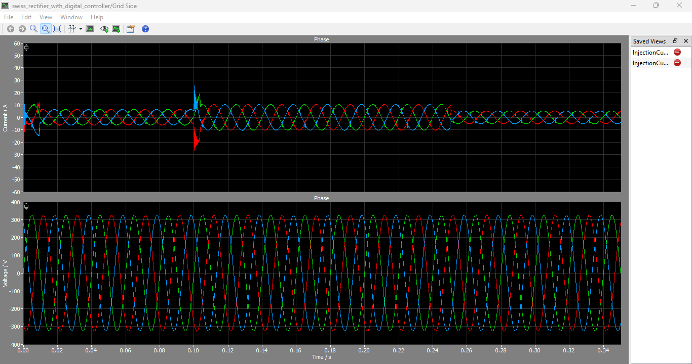
Figure 6: Three phase Grid connected Input voltage and current graphs generated in PLECS simulation
Figure 6 shows the three-phase grid-connected input voltage and current waveforms obtained from the PLECS simulation. The results demonstrate that the input currents closely follow the sinusoidal shape of the grid voltages, indicating effective power factor correction by the Swiss Rectifier. The current waveforms exhibit reduced harmonic distortion due to the combined effect of the injection network and LC input filter. During transient conditions such as startup and reference changes, minor oscillations are observed, which settle quickly as the control system reaches steady state. These results confirm the effectiveness of the digital control strategy in achieving near-unity power factor operation [1], [2].
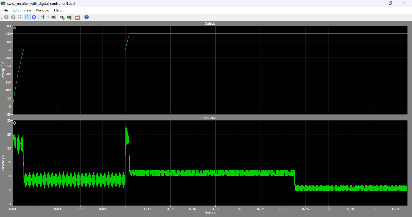
Figure 7: Output load voltage and current graphs generated by Swiss Rectifier in PLECS
You can download the Project files here: Download files now. (You must be logged in).
Figure 7 presents the output load voltage and current waveforms generated by the Swiss Rectifier system in PLECS simulation. The output voltage is regulated to follow the reference value with minimal steady-state error, demonstrating effective performance of the outer voltage control loop. The load current response shows stable behavior under both steady-state and transient conditions, including reference voltage changes and load variations. The fast settling time and low ripple content indicate proper tuning of the inner current controller and effective energy transfer through the DC-link capacitor. Overall, the results validate the ability of the Swiss Rectifier to maintain stable DC output regulation under dynamic operating conditions [1], [3].
The simulation is conducted under three operating conditions:
A. Startup Behavior
At startup, the output capacitor is initially uncharged, resulting in high inrush current. The LC filter resonates due to sudden energization, producing transient oscillations in grid currents. The system stabilizes within approximately 10 ms.
B. Output Voltage Step Response
At t = 0.1 s, the reference DC voltage is increased from 350 V to 450 V. The controller responds by increasing the current reference, resulting in a controlled charging of the output capacitor. The system reaches a new steady state within 4 ms, demonstrating fast dynamic response.
C. Load Disturbance
At t = 0.25 s, the load is reduced by 50%. This causes the DC-link capacitor to discharge, temporarily increasing output voltage. The controller compensates by reducing current injection, restoring steady-state conditions within 2 ms.
D. Switching Strategy Comparison
Two switching strategies are evaluated:
- Phase-shifted carrier modulation
- Minimal injection current ripple strategy
The phase-shifted method minimizes DC inductor ripple, while the minimal injection method reduces grid-side ripple in the injected phase current. Simulation results show that phase-shifted carriers provide smoother DC current, whereas the alternative strategy improves grid current quality.
VII. Power Quality and Performance Analysis
The Swiss Rectifier demonstrates significant improvements in power factor and harmonic reduction. The injection network ensures that all three phases contribute to energy transfer, reducing non-conducting intervals typical in diode rectifiers.
The LC input filter effectively attenuates high-frequency switching harmonics, ensuring compliance with electromagnetic compatibility (EMC) standards [2]. The digital control system maintains stable operation under varying load conditions and grid disturbances.
VIII. Advantages and Limitations
Advantages
- High power factor operation
- Reduced input current harmonics
- Buck-type voltage control capability
- Fast dynamic response due to digital PI control
- Reduced EMI due to LC filtering
Limitations
- Increased control complexity
- Requirement for accurate grid synchronization
- Additional switching losses in injection network
- Sensitivity to parameter variations in LC filter
IX. Future Work
Future improvements may include:
- Implementation of model predictive control (MPC) for improved dynamic performance
- Optimization of switching patterns using AI-based control strategies
- Hardware implementation using DSP or FPGA platforms
- Extension to bidirectional power flow for energy storage integration
- Reduction of switching losses using soft-switching techniques
X. Conclusion
This paper presented a detailed modeling, simulation, and control analysis of a 5 kW Swiss Rectifier using PLECS. The system integrates a diode bridge rectifier, injection network, and LC input filter with a cascaded digital control strategy. Two key control equations governing modulation index and duty cycle generation were derived and analyzed. Simulation results confirmed that the Swiss Rectifier achieves stable DC voltage regulation, improved power quality, and fast transient response under load variations.
The study demonstrates that digital control combined with advanced rectifier topologies provides a viable solution for high-efficiency AC–DC conversion in modern power electronic applications such as electric vehicle charging and renewable energy systems.
References
[1] T. B. Soeiro, T. Friedli, and J. W. Kolar, “Swiss Rectifier – A novel three-phase buck-type PFC topology for electric vehicle battery charging,” Proc. IEEE APEC, pp. 2617–2624, 2012.
[2] T. Nussbaumer, M. L. Heldwein, and J. W. Kolar, “Differential mode input filter design for a three-phase buck-type PWM rectifier,” IEEE Trans. Ind. Electron., vol. 53, no. 5, pp. 1649–1661, Oct. 2006.
[3] J. Rodriguez et al., “Multilevel converters: An enabling technology for high-power applications,” IEEE Trans. Ind. Electron., 2002.
[4] M. P. Kazmierkowski and L. Malesani, “Current control techniques for three-phase voltage-source PWM converters,” IEEE Trans. Ind. Electron., 1998.
You can download the Project files here: Download files now. (You must be logged in).







Responses