

A High-Efficiency Series Capacitor Buck Converter with Constant On-Time Control: Modeling, Simulation, and Performance Analysis Using PLECS

Author: Waqas Javaid
Abstract
This paper presents the modeling, simulation, and performance analysis of a two-phase series capacitor buck converter employing constant on-time (COT) control, implemented in the PLECS simulation environment. The series capacitor buck converter is an advanced DC–DC topology that integrates a switched-capacitor voltage divider with a multiphase buck converter, enabling high step-down conversion ratios while maintaining improved efficiency and reduced switching stress. The inherent 2:1 voltage division provided by the series capacitor reduces the effective voltage stress across switching devices, making the topology suitable for low-voltage point-of-load (POL) applications.
The converter operation is regulated using a constant on-time control strategy, which maintains a fixed switch on-duration while dynamically adjusting the off-time based on output voltage ripple feedback. This results in variable switching frequency operation, enabling fast transient response and simplified control architecture. The model demonstrates natural inductor current balancing without the need for additional current sensing or active current-sharing loops.
Simulation results obtained from PLECS confirm stable operation under a 12 V input supply, achieving an output voltage of approximately 1.2 V (one-tenth of the input voltage). The study further validates that switch node voltages are effectively clamped to half the input voltage, significantly reducing switching losses. Additionally, the system maintains balanced inductor currents even under inductance mismatch conditions, confirming the robustness of the topology.
Introduction
The demand for high-efficiency, high-density DC–DC converters has increased significantly due to modern applications in microprocessors, telecommunications, embedded systems, and renewable energy systems. These applications require low output voltages with high current levels, often derived from relatively higher input voltages. Conventional buck converters face limitations in achieving extremely high step-down ratios due to increased switching losses, reduced duty cycle resolution, and thermal stress on switching devices.
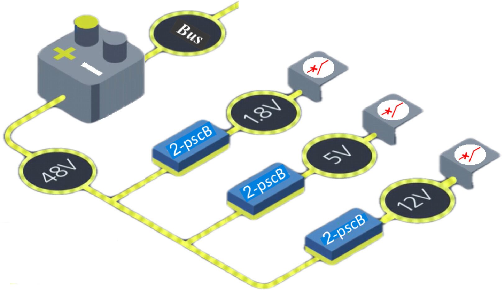
Figure A: Two-phase series-capacitor buck DC-DC converter
Figure A presents the two-phase series-capacitor buck DC-DC converter with Bus to 48 V to point-of-load (PoL) telecom power system. To address these limitations, advanced converter topologies such as switched-capacitor converters and multiphase buck converters have been extensively studied. Among these, the series capacitor buck converter (SCBC) has emerged as a promising solution that combines the benefits of both approaches. By integrating a flying (series) capacitor into a multiphase buck structure, the converter achieves an inherent voltage reduction mechanism that effectively divides the input voltage before processing it through the output stage. This significantly reduces voltage stress across semiconductor devices and improves overall conversion efficiency.
The SCBC topology, as presented in literature [1], introduces a natural 2:1 voltage division through the series capacitor, allowing the switching nodes to operate at approximately half of the input voltage. This characteristic not only reduces switching losses but also improves electromagnetic performance and device reliability. Additionally, the multiphase structure inherently balances inductor currents without requiring complex current-sharing control loops, making the system simpler and more robust.
Control strategy plays a critical role in ensuring stable operation of such converters. Conventional PWM-based control schemes may face challenges in maintaining regulation at extremely low duty cycles. Therefore, constant on-time (COT) control has gained attention as an effective alternative, particularly for low-voltage, high step-down applications. In COT control, the switch on-time remains fixed while the off-time varies depending on output voltage ripple feedback, resulting in a variable switching frequency operation that enhances transient response and simplifies controller design [3].
This paper focuses on the implementation of a two-phase series capacitor buck converter using constant on-time control in the PLECS simulation environment. The objective is to analyze its steady-state behavior, voltage conversion characteristics, inductor current balancing, and switching node stress reduction. The study provides detailed insights into converter performance under nominal and perturbed conditions, demonstrating its suitability for modern point-of-load power applications.
Literature Review
The evolution of high step-down DC–DC converters has been driven by increasing requirements for low-voltage, high-current power delivery in modern electronic systems. Traditional buck converters, while widely used, face significant limitations when operating under very low duty cycles. These limitations include increased switching losses, poor efficiency at high conversion ratios, and difficulties in maintaining stable regulation due to narrow control resolution.
To overcome these issues, switched-capacitor converters (SCCs) and hybrid multiphase architectures have been extensively investigated in recent literature. Switched-capacitor techniques enable discrete voltage conversion ratios by periodically reconfiguring capacitor connections, eliminating the need for inductors in some cases. However, pure SCCs suffer from high output ripple, limited load regulation capability, and lack of smooth control flexibility [1].
Multiphase buck converters, on the other hand, improve current handling capability and reduce output ripple by distributing the load across multiple interleaved phases. They also improve thermal performance and transient response. However, conventional multiphase buck converters still rely on full input voltage switching stress and require complex current sharing mechanisms to maintain balanced operation [2].
The series capacitor buck converter (SCBC) addresses these limitations by combining the advantages of both switched-capacitor and multiphase buck converter architectures. As reported in [1], the introduction of a series (flying) capacitor creates an inherent 2:1 voltage division at the input stage. This reduces the effective voltage seen by switching devices and improves overall efficiency. Furthermore, the topology naturally balances inductor currents due to its symmetrical structure, eliminating the need for additional current sensing or active balancing loops.
Recent studies have also highlighted the importance of advanced control strategies for such hybrid converters. While traditional voltage-mode or current-mode PWM control can be used, they are less effective at extremely low duty cycles where resolution and stability become challenging. Constant on-time (COT) control has emerged as a robust alternative, particularly for point-of-load (POL) converters. In COT control, the switch on-time is fixed, and regulation is achieved by modulating the off-time based on output voltage ripple feedback [3]. This method enhances transient response and reduces controller complexity, making it highly suitable for modern digital loads with fast dynamic behavior.
PLECS-based simulation environments have become widely used for validating power electronic converters due to their ability to accurately model switching behavior, magnetic components, and control systems in a unified platform. Prior works demonstrate that PLECS is particularly effective in analyzing multiphase converters and switched-capacitor hybrids due to its event-driven simulation capability and fast convergence characteristics.
Despite these advancements, challenges remain in optimizing SCBC performance under varying load conditions, component tolerances, and high-frequency operation. This paper builds upon existing literature by providing a detailed PLECS-based implementation of the SCBC with constant on-time control, focusing on inductor current balancing, switching stress reduction, and low-voltage regulation accuracy.
Series Capacitor Buck Converter Topology
The series capacitor buck converter is a hybrid DC–DC topology that integrates a switched-capacitor network with a two-phase buck converter structure. Its primary objective is to achieve high-efficiency step-down conversion by reducing the effective input voltage before it is processed by the switching stage.
3.1 Operating Principle
The topology consists of two interleaved switching phases, each driving an inductor. A series (flying) capacitor is placed between the input and switching nodes, which naturally charges to approximately half of the input voltage under steady-state conditions. As a result, each switching node (VSWA and VSWB) experiences only half of the input voltage stress.
This voltage division significantly reduces switching losses and improves device reliability. The output stage behaves similarly to a conventional buck converter but with an effective input voltage of Vin/2V_{in}/2Vin/2, allowing higher step-down ratios without extreme duty cycle constraints.
3.2 Voltage Conversion Characteristics
In steady-state operation, the converter exhibits a natural voltage scaling behavior governed by its internal capacitor charge balance and duty cycle limitation. Due to the structural symmetry and capacitor voltage balancing, the converter inherently maintains:
- Series capacitor voltage ≈ Vin/2
- Switch node voltage stress ≈ Vin/2
- Output voltage significantly lower than input voltage
This makes the topology particularly suitable for point-of-load applications requiring sub-2 V outputs from 10–12 V inputs.
3.3 Advantages of the Topology
The series capacitor buck converter offers several key advantages:
- Reduced switching voltage stress across MOSFETs
- Improved conversion efficiency at high step-down ratios
- Natural inductor current balancing without sensing circuits
- Reduced electromagnetic interference (EMI) due to lower voltage swings
- Scalability to multiphase operation for high current applications
However, the topology also introduces design constraints such as limited maximum duty cycle and dependency on capacitor voltage ripple for proper operation. These constraints must be carefully managed through appropriate control design, which is addressed in the next section.
Constant On-Time Control Strategy
The control of the series capacitor buck converter is implemented using a Constant On-Time (COT) control scheme, which is particularly suitable for high step-down, low duty-cycle DC–DC converters. Unlike conventional fixed-frequency PWM control, COT control maintains a constant switch on-duration while allowing the off-time to vary depending on the feedback signal. This results in a variable switching frequency operation that improves transient response and simplifies loop compensation.
In the studied converter, the output voltage is regulated by comparing the feedback voltage Vfb, which contains ripple information from the output capacitor, with a reference voltage V∗ref. When the feedback voltage falls below the reference threshold, the controller triggers a switching pulse of fixed duration t_on. After this on-time interval, the switch is turned off and remains off until the feedback condition again demands activation.
The basic operation of the COT controller can be mathematically described using the duty-cycle relationship:
4.1 Minimum Off-Time Protection
To prevent inductor saturation and excessive switching frequency during transient conditions, a minimum off-time block is incorporated. This ensures that the switch remains off for a predefined minimum duration even if the feedback voltage requests immediate reactivation. This mechanism stabilizes operation under sudden load changes and prevents subharmonic oscillations.
4.2 Feedback Ripple Requirement
A key requirement of COT control is the presence of output voltage ripple. In this converter, the ripple is naturally generated by the Equivalent Series Resistance (ESR) of the output capacitor. The ripple signal is essential because it acts as a carrier for the comparator-based control loop. Without sufficient ripple, the controller may exhibit jitter or unstable switching behavior.
You can download the Project files here: Download files now. (You must be logged in).
PLECS Modeling Methodology
The converter is implemented in the PLECS simulation environment, which provides accurate time-domain modeling of switching converters, magnetic components, and control systems. The model is structured into two main subsystems:
5.1 Power Stage Modeling
The power stage consists of:
- Two interleaved buck phases
- Series (flying) capacitor Cser
- Output filter capacitor Cout
- Resistive load Rout
- Inductors L1 and L2
The series capacitor naturally charges to approximately half of the input voltage under steady-state conditions, enabling reduced voltage stress across switching nodes VSWA and VSWB. Each inductor operates in interleaved fashion, sharing the load current equally.
Parasitic resistances such as inductor ESR RL, capacitor ESR RCser, and output capacitor resistance RCout are included to improve model realism and to ensure correct ripple generation for COT operation.
5.2 Control System Implementation
The control architecture consists of:
- Voltage feedback network
- Comparator-based COT modulator
- Fixed on-time generator
- Minimum off-time protection block
- Logic gate-based switching driver (AND/OR structure)
The feedback voltage Vfb is scaled from the output voltage Vout using a resistive divider. This signal is compared with the reference voltage V∗ref. When Vfb<V∗ref, a trigger signal is generated, initiating a constant on-time pulse.
The switching logic ensures proper gating of the four MOSFETs in the two-phase structure, maintaining interleaving and preventing shoot-through conditions.
5.3 Simulation Setup
The simulation is configured with the following key parameters:
- Input voltage: 12 V
- Target output voltage: ~1.2 V (1/10 of input)
- Series capacitor voltage: ~6 V (1/2 of input)
- Inductance: 220 nH (with mismatch test at 110 nH)
- Simulation time: 4 ms steady-state observation
The system is initialized to ensure stable startup conditions before enabling COT operation. The model also includes transient test scenarios where inductance mismatch is introduced to evaluate automatic current balancing performance.
Simulation Results and Discussion
The performance of the two-phase series capacitor buck converter was evaluated using the PLECS simulation environment under steady-state and transient operating conditions. The converter was tested with a 12 V DC input supply, and the desired output voltage was set to approximately 1.2 V, corresponding to a 10:1 step-down ratio. The results validate the effectiveness of the topology in achieving high-efficiency voltage conversion while maintaining balanced operation across phases.
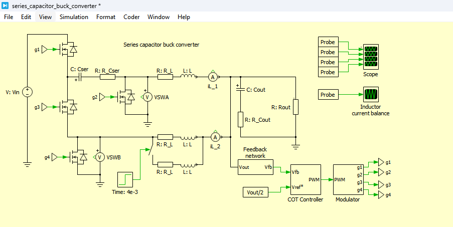
Figure 1: Series Capacitor buck converter Model development using PLECS
Figure 1 illustrates the complete implementation of the series capacitor buck converter developed in the PLECS simulation environment. It shows the two-phase interleaved structure, including the input source, switching network, series capacitor, inductors, and output filter. The model demonstrates how the flying capacitor is integrated between phases to achieve inherent voltage division and reduced switch stress, forming the basis of the converter operation.
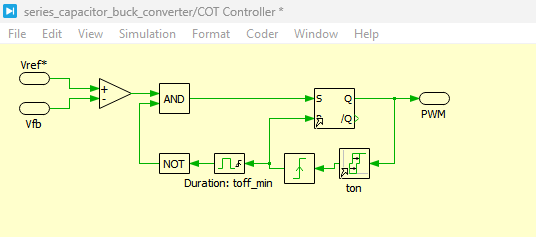
Figure 2: Constant on Time circuit in PLECS Simulation
Figure 2 presents the constant on-time (COT) control circuit implemented in PLECS. It includes the comparator-based feedback loop, reference voltage, and fixed on-time pulse generator. The controller regulates the output voltage by maintaining a constant switch ON duration while adjusting the OFF time based on feedback ripple, ensuring stable output regulation under varying load conditions.
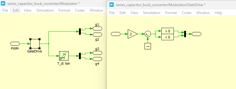
Figure 3: Modular and Gate driver circuit in PLECS
You can download the Project files here: Download files now. (You must be logged in).
Figure 3 shows the modulator and gate driver logic used to generate switching signals for the two-phase converter. The circuit includes logical AND/OR blocks, PWM generation, and interleaving control for proper switching coordination of all power switches. This ensures correct phase shifting and prevents shoot-through conditions while maintaining synchronized operation of both converter phases.
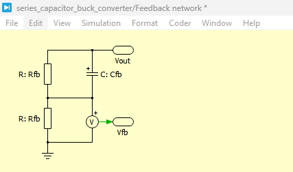
Figure 4: Feedback network circuit developed in PLECS
Figure 4 illustrates the voltage feedback network used for sensing and scaling the output voltage. A resistive divider reduces the output voltage to a suitable feedback level for the controller. This feedback signal (Vfb) is compared with the reference voltage (Vref*) to regulate the converter output through the COT control mechanism.
6.1 Steady-State Performance
Under steady-state conditions, the converter demonstrates stable voltage regulation and proper energy transfer between the input, series capacitor, and output stage. The series capacitor voltage naturally settles at approximately 6 V, which is half of the input voltage, confirming the theoretical voltage division principle of the topology.
The output voltage stabilizes at approximately 1.2 V, with minimal ripple due to the combined effect of the output capacitor and ESR-induced ripple required for constant on-time (COT) control. The switch node voltages VSWA and VSWB are effectively clamped to around 6 V, significantly reducing voltage stress on the switching devices and improving overall efficiency.
The inductor currents in both phases remain well-balanced, confirming the inherent current-sharing capability of the topology without requiring external current sensing or balancing control loops. This is a key advantage of the series capacitor buck converter, especially in high-current point-of-load applications.
6.2 Inductor Current Balancing Under Parameter Mismatch
To evaluate robustness, a perturbation test was conducted where the inductance of one phase was reduced from 220 nH to 110 nH at t = 4 ms. Figure 5 represents a significant component mismatch scenario that typically leads to uneven current distribution in conventional multiphase converters.
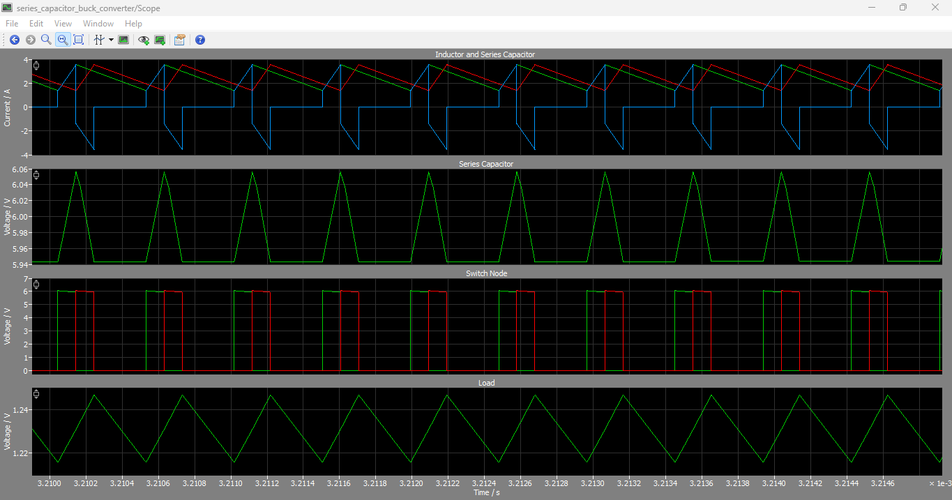
Figure 5: Simulation result inductor and series capacitor current, Series capacitor voltage, Switch Node Voltages and Load voltage in steady-state operation
Figure 5 presents the steady-state waveforms of the converter, including inductor currents, series capacitor voltage, switch node voltages, and output voltage. The results confirm stable operation, with the series capacitor maintaining approximately half the input voltage, switch nodes clamped at this level, and the output regulated at a low DC value with minimal ripple.
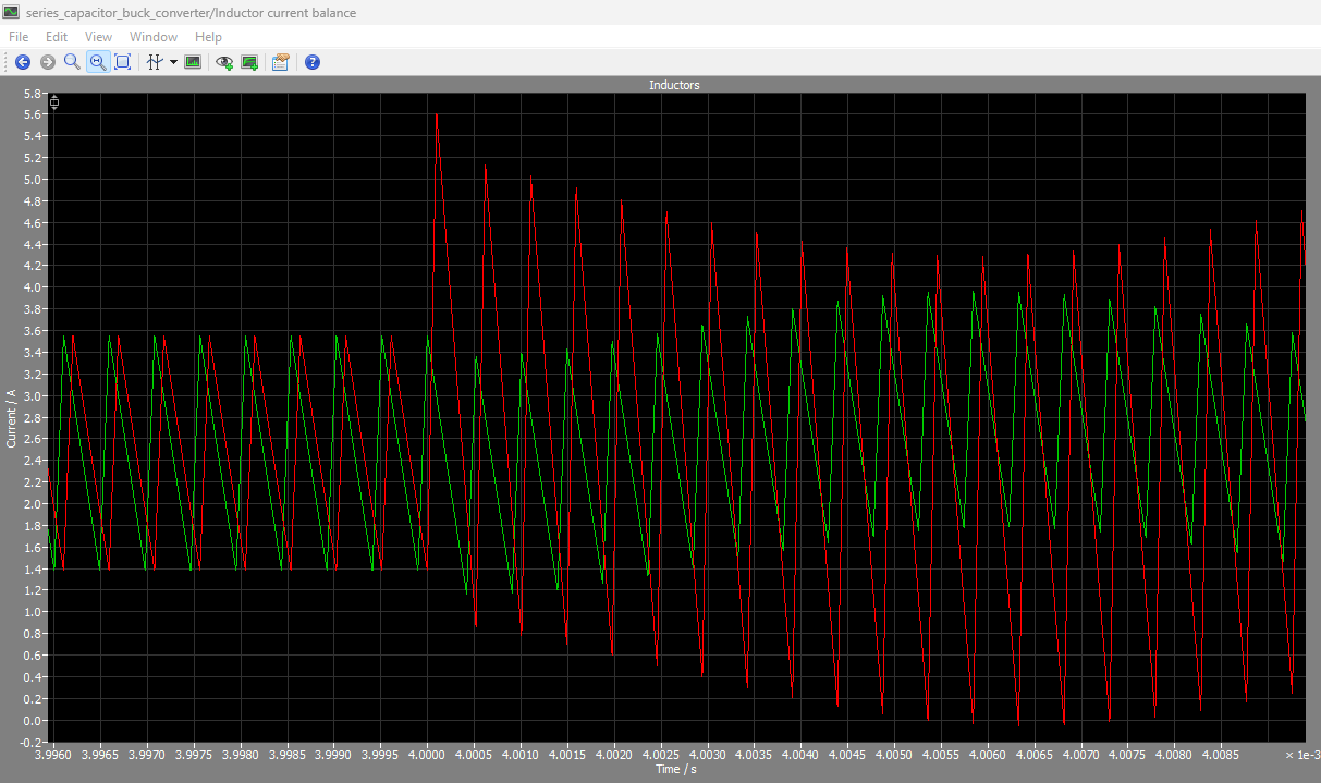
Figure 6: Inductor’s current output graphs in PLECS
You can download the Project files here: Download files now. (You must be logged in).
Figure 6 shows the inductor current waveforms for both phases of the converter. The results demonstrate that despite parameter variations, the inductor currents remain balanced over time due to the inherent current-sharing capability of the topology. This confirms stable multiphase operation without requiring additional current balancing control loops.
However, the simulation results presented in figure 6 confirm that the average inductor currents remain balanced even after the inductance variation. This demonstrates the self-balancing nature of the topology, where energy redistribution through the series capacitor compensates for inductance mismatch.
6.3 Voltage Waveform Behavior
The simulation waveforms confirm the following key observations:
- Series capacitor voltage remains stable at ~6 V
- Switch node voltages are limited to half of input voltage
- Output voltage is tightly regulated at ~1.2 V
- Minimal transient overshoot is observed during startup
These results validate that the topology successfully reduces voltage stress and improves switching efficiency.
6.4 Switching Behavior and Efficiency Implications
The constant on-time control introduces variable switching frequency operation, which helps improve transient response and reduces switching losses under light-load conditions. Since the switch nodes operate at reduced voltage levels, the switching loss component is significantly lower compared to conventional buck converters operating directly from 12 V input.
Additionally, the multiphase operation reduces output current ripple and distributes thermal stress evenly across switching devices, improving system reliability.
6.5 Key Performance Summary
The overall simulation results confirm the following performance advantages:
- 2:1 inherent voltage reduction through series capacitor
- Output voltage regulation at 1/10 of input voltage
- Self-balancing inductor currents without control loops
- Reduced switch stress (limited to half input voltage)
- Robust operation under inductance mismatch
- Fast transient response using COT control
Conclusion
This paper presented a comprehensive modeling and performance analysis of a two-phase series capacitor buck converter (SCBC) implemented using constant on-time (COT) control in the PLECS simulation environment. The study focused on evaluating the converter’s ability to achieve high step-down voltage conversion, maintain current balance, and reduce switching stress under steady-state and transient operating conditions.
The SCBC topology demonstrated a significant advantage over conventional buck converters by incorporating a series (flying) capacitor that naturally divides the input voltage into approximately half before being processed by the switching stage. This inherent voltage division reduces the effective voltage stress on the switching devices, where both switch nodes were observed to operate at approximately 50% of the input voltage (6 V for a 12 V input). As a result, switching losses and device stress are significantly reduced, improving overall efficiency and reliability.
The constant on-time control strategy provided a simple yet effective regulation mechanism for maintaining a stable output voltage. By fixing the on-time duration and varying the off-time based on output voltage ripple feedback, the converter achieved fast dynamic response and stable regulation at a low output voltage of approximately 1.2 V, corresponding to one-tenth of the input voltage. The inclusion of minimum off-time protection ensured stable operation under transient load conditions and prevented excessive switching frequency.
A key finding of this study is the inherent current balancing capability of the SCBC topology. Even when a significant inductance mismatch was introduced (220 nH to 110 nH), the average inductor currents remained balanced. This confirms that the topology does not require additional current sensing or active current-sharing control loops, simplifying the overall control design.
The PLECS simulation results validated the theoretical expectations, showing stable voltage regulation, reduced ripple, and robust dynamic behavior. Overall, the SCBC with COT control proves to be a highly suitable solution for modern point-of-load (POL) applications, particularly in systems requiring high step-down ratios, high efficiency, and compact power delivery architectures.
Future work may include experimental hardware validation, thermal performance analysis, and optimization of switching frequency behavior under wide load variations.
References
[1] P. Shenoy, “Design of a high-frequency series capacitor buck converter,” Texas Instruments Power Supply Design Seminar, 2016/2017.
[2] P. Shenoy, “Introduction to the Series Capacitor Buck Converter,” Texas Instruments Application Report SLVA750A, Texas Instruments, 2017.
[3] R. Mammano, “Switching control algorithms,” in Fundamentals of Power Supply Design, 1st ed., Texas Instruments, 2001.
You can download the Project files here: Download files now. (You must be logged in).






Responses