

Welding Inverter Design Calculator
Size a two-switch forward welding inverter: transformer turns and copper, output choke, switch currents and losses, mains demand, and the arc load characteristic.

This welding inverter design calculator sizes the electrical power stage of a two-switch forward converter. It is for engineers comparing magnetic and semiconductor choices, students studying isolated converters, and experienced electronics designers checking an early specification. It brings welding inverter transformer calculation, output choke sizing and mains demand into one transparent calculation sheet.
Start with the required welding current and the arc voltage characteristic. The default linear characteristic gives 26.4 V at 160 A, matching a published manual metal arc voltage endpoint. You can change its intercept and slope to represent another intended load. The voltage-capability chart shows whether the chosen transformer ratio and available switching duty can support that load at minimum and maximum DC bus voltage. It is a steady design comparison; a real arc and its current controller have dynamic behavior.
Enter the loaded DC bus valley and maximum bus separately. These depend on mains tolerance, rectification, bulk-capacitor ripple and any power factor correction stage. Specify the switching frequency and keep maximum PWM duty below one half so the transformer can reset. The two primary switches turn on together and carry the same branch current. The waveform player illustrates power transfer, negative reset voltage and continued choke freewheeling over a slowed switching period.
Next enter effective core and window areas, allowable flux excursion, magnetizing inductance, current density and copper temperature. The calculator rounds transformer turns upward, estimates bare copper areas, checks window fill and includes hot winding resistance in the duty calculation. Its forward-converter flux excursion must not be confused with the peak flux of a balanced bridge transformer.
For the output choke, compare chosen inductance with the ripple target. Results include current valley and peak, stored energy, suggested turns, copper area and equivalent total gap. This gap represents an ideal reluctance requirement; it does not specify how to grind or assemble a core. Fringing, distributed-gap behavior and inductance under DC bias require separate verification.
The loss budget combines IGBT conduction and switching, transformer copper, output rectifiers, choke, leads and entered core and miscellaneous allowances. Replace illustrative energy and loss inputs with device data or measurements. Mains current uses true power factor and front-end efficiency. Welding duty cycle affects average power and a cycle heating estimate, while component peak and RMS stresses remain based on active welding.
This is a design calculator, not a build guide or a compliance assessment. It does not design ignition, short-circuit protection, current-loop compensation, cooling, isolation or safe no-load voltage control. Mains and high-current work requires qualified engineering. IEC 60974-1:2021 names the relevant welding-power-source safety framework; check against the standard in force. Mains installation work belongs to a qualified person.
How it is calculated
This is a continuous-conduction, two-switch forward sizing model. Erickson and Maksimović, Fundamentals of Power Electronics, 3rd ed. (2020), provides the steady-state volt-second balance, RMS-current, loss and magnetic-design framework. The equations below are derived here; ST AN4638, pp.3–4 and Appendix A, supplies the welding topology and device-stress context.
With , and , inductor volt-second balance gives
The editable arc line is . Defaults reproduce the MMA voltage endpoints in ST AN4638 Table 2, p.6; this is a design load characteristic, not a measured plasma model. The chart compares it with maximum-duty voltage capability using fixed turns and winding resistances. It does not predict a constant-current controller characteristic.
Primary turns are rounded upward from . The secondary is rounded upward to meet both approximate loaded duty and no-load pulse headroom at minimum bus. Copper voltage drop is then included in the actual duty check. Failure of that check requires revising the inputs. Forward flux is unipolar excursion, unlike the balanced bridge peak-flux convention in Transformer Design. Its current-density, bare-copper window budget, IACS resistivity, hot-resistance and skin-depth equations are reused and adapted here. Copper areas include a 10% allowance; the RMS triangle inequality bounds the primary sizing current including magnetizing current.
For ideal reset diodes, . Primary current rises linearly from to ; a pulse with endpoints has . Secondary load current flows only during on-time. The primary winding also carries the decreasing magnetizing reset pulse, adding to its mean-square current. That reset current flows through the clamp diodes, not through the IGBTs; their RMS current includes only the on-time pulse. The primary copper sizing bound allows both on and reset magnetizing intervals. Parallel switch devices share current equally.
Secondary diode stress is checked by interval: the forward rectifier blocks the reset plateau , while the freewheel diode blocks the on-state pulse . Their maximum is the ideal reverse-voltage baseline, consistent with the bus-based stress in onsemi AND8373/D, equation 31. Reset-diode drops and transient leakage/recovery overshoot need separate allowance; this plateau estimate is not a selected device rating.
Choke ripple is . The high-bus corner sizes inductance and peak energy. Choke turns follow ; is an equivalent total reluctance gap. A physical gap requires core-reluctance and fringing corrections; this value is not a machining instruction.
Losses are evaluated at both DC-bus endpoints. IGBT conduction uses constant hot ; switching energy uses equal on/off weighting and linear current/voltage scaling of the entered per-device . Transformer copper, output diode conduction, choke DC resistance, leads, transformer core and other allowances are included. Enter choke core loss and excess AC copper loss in the other-loss allowance. Lead heating conservatively uses high-bus ripple at both corners. The larger endpoint budget feeds mains power through the entered front-end efficiency and true power factor.
Welding duty changes time-averaged arc power and the heating-equivalent mains estimate . It never reduces switch, magnetic or instantaneous winding ratings.
Assumptions
- One isolated forward secondary, one forward rectifier and one freewheel diode; steady positive choke current and fixed switching frequency. Both primary switch positions conduct together.
- The minimum and maximum DC-bus voltages are independent engineering inputs. Determine loaded valleys, high-line peaks or PFC limits separately; mains voltage alone does not establish them.
- Custom magnetic geometries are illustrative, not catalogue parts. Flux ceilings, copper current density, window allowance, loss factors and energy inputs must be chosen for the actual materials and temperature.
- Primary RMS current includes the ideal magnetizing reset pulse but not a separately resolved core-loss excitation component. Core loss is an entered power allowance; its small waveform contribution must be included in a detailed design. The transformer starts each cycle at a reset baseline. Remanence, flux walking, leakage, startup imbalance and saturation curvature are excluded. Maximum-duty high-bus excitation is checked even though operating duty is lower.
- The resistance-only duty model uses mean load current and excludes magnetizing-current voltage drop and within-cycle resistive distortion. Ripple assumes a constant output terminal voltage over one period.
- Choke hot DC resistance is supplied independently. Suggested turns, copper area and equivalent gap do not verify a realizable core, winding layout or resistance.
- Switching energy is a local scaling estimate. Equal on/off weights, linear scaling and equal sharing must be checked against device curves or measurements. Recovery energy must be counted once. Clamp losses, gate drives and other losses belong in the separate allowance.
- The waveform player is a slowed-down illustration of the low-bus corner. Current and flux remain calculated at the selected electrical operating point; no feedback dynamics are simulated.
Where it applies
Use for preliminary engineering comparisons of CCM IGBT two-switch forward welding power stages. The default case is approximately 4.2 kW at 160 A. Endpoint loss budgets do not guarantee that an interior bus voltage cannot produce a larger loss. Magnetic loss, switching energies, hot resistances and cooling require independent confirmation.
The no-load target only sets necessary secondary pulse headroom. At no load the CCM gain law fails, and an output capacitor can charge toward the secondary pulse peak. This tool does not establish actual open-circuit voltage, safe touch voltage or voltage-reduction-device behavior. Ignition, arc extinction, short circuits, anti-stick/hot-start functions, current-loop stability, output-capacitor dynamics, leakage spikes, transient SOA, inrush, bulk capacitance and EMC are outside scope.
Mains voltage, stored DC-link energy and welding current can cause fatal shock, burns and fire. This is a design calculation, not a build guide. IEC 60974-1:2021, edition 6, specifies safety and performance requirements for welding power sources; check against the standard in force and its applicable national adoption. No standards tables are reproduced and no compliance or nameplate rating is certified here. Isolation, creepage, clearance, protective earthing, discharge provisions, output-voltage limits, protective devices and thermal tests require separate qualified assessment. Mains installation work belongs to a qualified person. The cycle RMS estimate does not select a supply cable, plug, breaker or fuse.
References
- R. W. Erickson and D. Maksimović, Fundamentals of Power Electronics, 3rd ed., Springer, 2020. Steady-state converter analysis, losses and magnetics. DOI: 10.1007/978-3-030-43881-4. https://doi.org/10.1007/978-3-030-43881-4
- STMicroelectronics, AN4638, Welding machines: V and HB series IGBTs on two-switch forward converters, Rev.1, January 2015; pp.3–4, Table 2 p.6, Appendix A pp.20–21. Attached s1. https://www.st.com/resource/en/application_note/an4638-welding-machines-v-and-hb-series-igbts-on-twoswitch-forward-converters-stmicroelectronics.pdf
- Texas Instruments, SLUS419C, UCC2850x/UCC3850x BiCMOS PFC/PWM Combination Controller, November 2001, p.21, equations 29–32. https://www.ti.com/lit/gpn/ucc38500
- National Bureau of Standards, Copper Wire Tables, Circular 31, 4th ed., 1956. IACS copper resistivity and temperature coefficient, also used by the catalog Transformer Design calculator. https://nvlpubs.nist.gov/nistpubs/Legacy/circ/nbscircular31e4.pdf
- IEC 60974-1:2021, edition 6, Arc welding equipment – Part 1: Welding power sources. Safety/performance scope; check against the standard in force. https://webstore.iec.ch/en/publication/64782
- Thierry Sutto, onsemi AND8373/D, 2 Switch-Forward Current Mode Converter, Rev.1, March 2010, printed p.2 (PDF p.3), equation 4: 350 V, 0.45 duty, 125 kHz, 13.4 mH and approximately 94 mA magnetizing peak. https://www.onsemi.com/pub/Collateral/AND8373-D.PDF
Inputs
| Input | Symbol | Unit | Default |
|---|---|---|---|
| Welding current Set the steady welding current; arc ignition and short circuits are excluded. | I_w | A | 160 |
| Arc characteristic intercept Editable linear load characteristic U = U₀ + r I; defaults reproduce ST AN4638 MMA voltage endpoints. | U_arc0 | V | 20 |
| Arc characteristic slope | r_arc | ohm | 0.04 |
| Controlled open-circuit voltage target Used only for secondary pulse-voltage headroom. Actual no-load voltage needs a separate control and protection design. | U_oc | V | 80 |
| Welding duty fraction Fraction of a 10-minute cycle spent welding. This is different from PWM switching duty. | X_w | 0.6 | |
| Single-phase mains voltage | V_ac | V | 230 |
| True mains power factor Use true power factor including distortion; a capacitor-input rectifier must not be assumed to have unity power factor. | PF_in | 0.85 | |
| Front-end efficiency Rectifier/PFC efficiency from mains to DC bus during welding. | eta_front | 0.96 | |
| Measured idle mains RMS current Used only for the cycle RMS current estimate; keep cooling and standby current included. | I_idle | A | 0.25 |
| Minimum loaded DC bus voltage Enter the actual valley under load, allowing for line tolerance and bulk-capacitor ripple. | V_lo | V | 250 |
| Maximum DC bus voltage Maximum steady bus including line or PFC tolerance. Transient spikes need additional margin. | V_hi | V | 360 |
| Switching frequency | f_sw | kHz | 50 |
| Maximum PWM duty fraction Both switches turn on together once per period; leave reset margin below 0.5. | D_lim | 0.45 | |
| Transformer effective core area | A_e | mm^2 | 600 |
| Transformer winding window area Area of one winding window; no catalogue core is implied by these custom geometry defaults. | A_w | mm^2 | 1600 |
| Allowed transformer flux excursion Unipolar ΔB from reset baseline, not the bipolar peak-flux value. Allow for remanence and temperature. | B_lim | T | 0.2 |
| Primary magnetizing inductance Use value at relevant excitation; primary magnetizing current is assumed to ramp from zero. | L_m | mH | 2 |
| Transformer mean turn length | MLT | mm | 190 |
| Winding design current density Continuous current-density choice; welding duty does not reduce the instantaneous sizing current. | J_cu | A/mm^2 | 5 |
| Allowed bare-copper window fill The remaining window must accommodate insulation, bobbin, strand packing and required spacings. | k_u | 0.4 | |
| Transformer AC/DC resistance factor Engineering estimate at switching frequency; skin depth alone does not predict proximity loss. | F_ac | 1.5 | |
| Assumed copper operating temperature One absolute temperature for transformer copper resistance; this calculator does not solve thermal rise. | T_cu | °C | 80 |
| Transformer core-loss allowance Enter measured or waveform-appropriate core loss at the actual flux, frequency and temperature. | P_core | W | 30 |
| Chosen output choke inductance Use incremental inductance at peak welding current, not the small-signal zero-bias value. | L_out | uH | 25 |
| Target peak-to-peak current ripple fraction | ripple_goal | 0.2 | |
| Choke effective core area | A_ch | mm^2 | 800 |
| Allowed choke peak flux density Select for actual material, temperature and DC bias. | B_ch_lim | T | 0.3 |
| Choke winding window area | A_ch_w | mm^2 | 2000 |
| Choke hot DC resistance Measured or independently estimated hot winding resistance. It is not derived from the equivalent gap. | R_ch | mohm | 3 |
| Total hot welding lead and contact resistance Loop resistance of both output leads and connections. | R_lead | mohm | 2 |
| IGBT on-state drop per device Constant hot VCE(sat) model. Replace with a conservative value at branch current. | V_ce | V | 1.6 |
| Parallel IGBTs per switch position Equal current sharing is assumed; each of the two series switch positions has this many devices. | n_par | 2 | |
| Forward rectifier drop | V_f | V | 1 |
| Freewheel diode drop | V_fw | V | 1 |
| Per-device turn-on plus turn-off energy Sum Eon + Eoff at the reference voltage and current. Include recovery in Eon if measured that way. | E_pair | mJ | 1 |
| Switching-energy reference collector current | I_ref | A | 40 |
| Switching-energy reference voltage | V_ref | V | 400 |
| Switch blocking-voltage design multiplier Headroom above the maximum bus, not proof of adequate transient clamping. | k_v | 1.3 | |
| Other DC-stage loss allowance Choke core and excess AC copper loss, gate drives, controls, clamp diodes and recovery not already included. Avoid counting recovery twice. | P_other | W | 20 |
| Switching-period phase ▶ Play a slowed-down low-bus switching period. Transformer reset and choke freewheeling continue after both switches turn off. | phase_pwm | 0.18 |
Results
With the default inputs above, the calc gives:
| Result | Value |
|---|---|
| Arc output power | 4,224 W |
| Transformer primary turns | 27 |
| Transformer secondary turns | 9 |
| PWM duty at minimum DC bus | 0.346 |
| PWM duty at maximum DC bus | 0.239 |
| Worst-case transformer flux excursion | 0.198 T |
| Minimum output choke inductance | 13.42 uH |
| Peak output choke current | 168.6 A |
| Suggested choke turns | 18 |
| Equivalent total choke gap | 13.03 mm |
| Peak collector current per IGBT | 28.52 A |
| RMS collector current per IGBT | 15.82 A |
| IGBT blocking-voltage target | 468 V |
| Worst checked total loss budget | 528.3 W |
| Arc efficiency from DC bus | 0.889 |
| Mains RMS current while welding | 25.32 A |
| Cycle-equivalent mains RMS current | 19.61 A |
| Welding time per 10-minute cycle | 6 min |
Checked against sources
Each case below was calculated by this calc and agrees with the value from its source (within the tolerance where one is shown).
ST AN4638 MMA200: 15 A arc endpoint
Source: STMicroelectronics AN4638 Rev.1 (2015), Table 2, p.6: MMA200 adjustment 15–190 A and output voltage 20.6–27.6 V. This checks the selected linear MMA load characteristic only, not plasma dynamics, magnetics or losses.
Inputs: Welding current = 15 A; the others as above.
| Result | Source | This calc |
|---|---|---|
| Arc voltage at selected current | 20.6 V | 20.6 V |
ST AN4638 MMA200: 190 A arc endpoint
Source: STMicroelectronics AN4638 Rev.1 (2015), Table 2, p.6: upper MMA200 operating endpoint, 190 A and 27.6 V. The characteristic is an editable design load line; this does not verify a real arc control loop.
Inputs: Welding current = 190 A; the others as above.
| Result | Source | This calc |
|---|---|---|
| Arc voltage at selected current | 27.6 V | 27.6 V |
ST AN4638 Appendix A: 6 kW primary current estimate
Source: ST AN4638 Rev.1, Appendix A p.21, published on-time average estimate 62.2 A for 6000 W input, 220√2 V bus and D=0.31. Here 6000 W arc output is deliberately interpreted as a lossless power-transfer lower bound to reproduce that input-power relation. The calculator's actual current includes loss and magnetizing contributions and must not be compared with the paper's ideal estimate. This case does not validate the source's rounded 72 A peak or 36 A per parallel IGBT.
Inputs: Welding current = 200 A; Arc characteristic intercept = 30 V; Arc characteristic slope = 0 Ω; Minimum loaded DC bus voltage = 311.1 V; Maximum DC bus voltage = 311.1 V; Maximum PWM duty fraction = 0.31; Switching frequency = 58 kHz; the others as above.
| Result | Source | This calc |
|---|---|---|
| Lossless lower bound on primary on-time average current | 62.2 ± 0.1 A | 62.209 A |
onsemi AND8373: magnetizing ramp and maximum on-time
Source: Thierry Sutto, onsemi AND8373/D Rev.1, March 2010, printed p.2 (PDF p.3), equation 4, and printed p.7 equation 29: a 350 V primary pulse lasting 3.6 µs, 13.4 mH magnetizing inductance and 94 mA peak. The voltage range is collapsed to that published low-line excitation corner and switch drop is set to zero. This checks magnetizing-current integration and timing, not the source's MOSFET loss model, transformer core or output ripple calculation.
Inputs: Welding current = 10 A; Arc characteristic intercept = 12 V; Arc characteristic slope = 0 Ω; Controlled open-circuit voltage target = 12 V; Minimum loaded DC bus voltage = 350 V; Maximum DC bus voltage = 350 V; IGBT on-state drop per device = 0 V; Switching frequency = 125 kHz; Primary magnetizing inductance = 13.4 mH; Chosen output choke inductance = 27 uH; the others as above.
| Result | Source | This calc |
|---|---|---|
| Magnetizing peak at maximum allowed excitation | 0.094 A | 0.09403 A |
| Maximum commanded on-time | 3.6 us | 3.6 us |
Related Resources
Related courses

IEC Electrical Schematics and Industrial Control Panels
5
Original price was: 42 €.21 €Current price is: 21 €.

Basic Electrical Controls & Diagram Reading
7
Original price was: 32 €.18 €Current price is: 18 €.
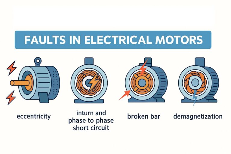
Modeling Electrical Motor Faults with FEM Simulation using ANSYS MAXWELL
3
Original price was: 50 €.15 €Current price is: 15 €.









Responses