

Real-Time SPI Communication Interface Implementation Using PLECS RT Box for Embedded Hardware-in-the-Loop Applications
Author: Waqas Javaid
Abstract
This paper presents the development and implementation of a real-time Serial Peripheral Interface (SPI) communication system using the PLECS RT Box platform. The project demonstrates a complete SPI Master-Slave communication architecture implemented within a single RT Box environment for embedded hardware-in-the-loop (HIL) applications. The developed model utilizes SPI Master and SPI Slave blocks available in the PLECS RT Box Target Support Package to establish synchronous serial communication between digital subsystems. The system validates high-speed bidirectional data transfer using sinusoidal, pulse, triangular, and constant signals transmitted between the SPI modules.
The developed model is divided into multiple functional subsystems including SPI transmission blocks, PWM synchronization modules, waveform generation circuits, and real-time monitoring interfaces. The SPI communication system is analyzed under two operating conditions: SPI transmission within a single RT Box model step and SPI transmission over multiple RT Box model steps. The implementation successfully demonstrates accurate signal reconstruction, synchronization, and real-time deterministic communication suitable for industrial embedded systems.
The proposed architecture also demonstrates synchronization between PWM generation and SPI transmission timing, allowing accurate analysis of timing delays and transmission intervals. Experimental validation through PLECS real-time simulation confirms correct implementation of SPI communication protocols, data framing, timing synchronization, and digital transmission accuracy. The developed framework provides an effective platform for testing embedded communication protocols, external ADC interfaces, and digital control systems without requiring complete physical hardware implementation.
I. Introduction
Serial Peripheral Interface (SPI) communication has become one of the most widely used synchronous serial communication protocols in embedded systems, industrial automation, motor drives, digital signal processing, and real-time control applications. Modern embedded controllers require fast and reliable communication methods to exchange information between sensors, microcontrollers, digital signal processors, analog-to-digital converters (ADCs), and peripheral devices. SPI communication offers high-speed full-duplex data transfer with low hardware complexity, making it highly suitable for real-time applications.
In industrial automation and power electronics systems, communication reliability and timing accuracy are critical requirements. Real-time controllers often interact with external devices through digital communication interfaces where delays, synchronization issues, and data corruption can severely affect system stability and performance. Therefore, testing communication systems under real-time conditions before practical deployment is extremely important for ensuring system robustness and operational reliability.
Hardware-in-the-loop (HIL) simulation has emerged as a highly efficient technique for validating embedded systems and communication architectures. HIL platforms allow real controllers and communication devices to interact with simulated plants in real time, reducing development risks and minimizing hardware prototyping costs. Among modern HIL platforms, the PLECS RT Box provides a highly efficient environment for implementing power electronic systems, embedded communication interfaces, and real-time digital controllers.
The SPI interface implemented in the PLECS RT Box enables deterministic communication using dedicated digital input and output channels. The RT Box includes integrated SPI Master and SPI Slave modules that support multiple parallel data channels, configurable clock polarity, configurable clock phase, and adjustable transmission timing. These features make the RT Box suitable for studying industrial communication systems and embedded digital interfaces.
In this project, a complete SPI communication demo model was developed using the PLECS RT Box platform. The implemented architecture establishes communication between SPI Master and SPI Slave subsystems located on the same RT Box. Various signals including sinusoidal, pulse, triangular, and constant waveforms are transmitted and received through the SPI interface. The developed model also demonstrates synchronization between SPI transmission and PWM generation signals to evaluate timing characteristics and communication delays.
The developed project further investigates two communication scenarios. The first scenario analyzes SPI communication occurring within a single RT Box simulation step. The second scenario evaluates SPI communication extending over multiple RT Box model steps. These investigations provide insight into timing synchronization, communication latency, and real-time data transfer performance under different sampling conditions.
The implementation additionally demonstrates advanced SPI applications involving external analog-to-digital converters. In the advanced configuration, the RT Box operates as an SPI Master connected to an external ADC evaluation board functioning as the SPI Slave. This setup enables real-time conversion of analog signals into digital SPI data streams for embedded monitoring applications.
The primary contribution of this work includes the development of a modular SPI communication framework suitable for embedded HIL validation, real-time digital interface testing, and industrial communication analysis. The proposed architecture provides flexibility for extending the system toward advanced communication protocols, distributed embedded systems, and real-time industrial automation applications.
II. System Overview
The developed SPI communication model consists of two primary communication entities: the SPI Master subsystem and the SPI Slave subsystem. Both subsystems are implemented using the integrated SPI communication blocks available in the PLECS RT Box Target Support Package. The overall architecture enables full-duplex communication where both the SPI Master and SPI Slave simultaneously transmit and receive data.
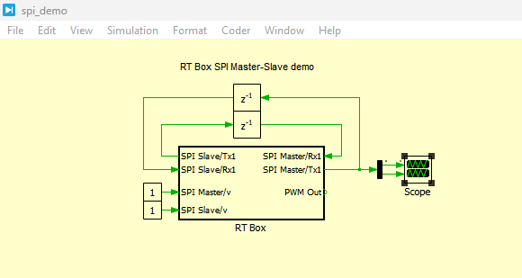
Figure 1: SPI System development with Master and Slave RT Box in PLECS schematics
Figure 1 presents the overall SPI system development implemented in PLECS, showing the complete Master–Slave communication architecture configured within the RT Box environment. The schematic illustrates how the SPI Master subsystem generates and transmits digital data streams, while the SPI Slave subsystem receives and responds using synchronized clock and chip select signals. It also highlights the bidirectional data flow between both modules along with the associated PWM synchronization and digital I/O connections. Overall, Figure 1 presents the foundational system structure used to establish real-time SPI communication for hardware-in-the-loop validation.
The SPI Master subsystem generates two digital signals consisting of a sinusoidal waveform and a pulse waveform. These signals are packed into two separate 16-bit digital words before transmission through the SPI data output channel. Similarly, the SPI Slave subsystem generates a triangular waveform and a constant digital value which are transmitted back toward the SPI Master subsystem through the reverse communication channel.
The SPI communication architecture utilizes dedicated digital input and output channels on the RT Box hardware. The SPI Master output lines are physically connected to the SPI Slave input lines through front-panel digital wiring connections. Likewise, the SPI Slave outputs are connected back to the SPI Master inputs, establishing complete bidirectional communication.
The entire communication process is synchronized using an SPI clock signal generated by the SPI Master module. A chip select (CS) signal controls the activation of the communication channel and ensures proper synchronization between the transmitting and receiving devices. The SPI protocol operates using a master-slave architecture in which the SPI Master controls communication timing while the SPI Slave responds according to the generated clock pulses.
To evaluate timing synchronization, the system additionally includes a PWM generation block configured with a 0.5 duty cycle. The PWM waveform is synchronized with the RT Box simulation step size and provides a timing reference for evaluating communication delays and SPI transmission intervals.
The developed model supports configurable communication timing parameters including clock polarity (CPOL), clock phase (CPHA), chip select delay, and SPI sample time. These adjustable parameters allow detailed investigation of different SPI operating conditions and synchronization requirements.
III. Mathematical Modeling
The SPI communication timing and synchronization behavior can be represented using the sampling relationship between the SPI transmission interval and the RT Box discretization step size. The communication sampling relationship is expressed by Equation (1) [1].

where:
- T_SPI represents the SPI transmission interval,
- N represents the number of RT Box simulation steps,
- Ts represents the RT Box discretization step size.
Equation (1) describes the synchronization relationship between the SPI communication interval and the real-time simulation sampling interval. In single-step communication mode, the SPI transmission interval equals one simulation step. In multi-step communication mode, the SPI transmission extends over multiple simulation steps.
The PWM synchronization waveform generated within the RT Box can be represented using the duty cycle expression shown in Equation (2) [1].
where:
- D represents the PWM duty cycle,
- T_ON represents the ON-state duration of the PWM pulse,
- T_SW represents the switching period of the PWM waveform.
The PWM synchronization signal is used as a timing reference to observe the exact timing relationship between SPI transmission intervals and RT Box model execution periods.
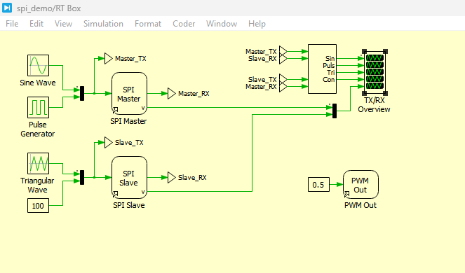
IV. SPI Master and Slave Configuration
The SPI Master subsystem is configured using the SPI1 communication module integrated into the RT Box hardware. The subsystem includes waveform generators, data-packing circuits, transmission logic, and synchronization controls. The sinusoidal and pulse waveforms are converted into digital words before transmission to the SPI Slave subsystem.
Figure 2: SPI Master and Slave development circuit in PLECS Simulation
You can download the Project files here: Download files now. (You must be logged in).
Figure 2 presents the detailed implementation of the SPI Master and SPI Slave development circuit in the PLECS simulation environment. It illustrates how the SPI Master subsystem is configured to generate digital data streams from input waveforms such as sine and pulse signals, which are then packed into transmission words and sent through the SPI interface. On the receiving side, the SPI Slave subsystem captures the transmitted data using synchronized clock and chip select signals, ensuring accurate reconstruction of the original information. Additionally, Figure 2 presents the bidirectional communication structure that enables simultaneous data exchange between both subsystems within the RT Box platform.
The SPI Slave subsystem is configured using the SPI2 communication module. The subsystem receives the SPI Master data stream while simultaneously transmitting triangular and constant digital signals back toward the SPI Master receiver. The SPI Slave follows the clock signal generated by the SPI Master to ensure synchronized communication.
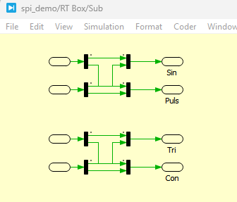
Figure 3: SPI Master and Slave signals emerge and generate the output signal waveforms
Figure 3 presents the SPI Master and Slave signal behavior along with the resulting output waveforms generated during real-time simulation. It illustrates how the transmitted signals from the SPI Master, including sine and pulse waveforms, are encoded into digital data and passed through the SPI communication channel. On the receiving side, the SPI Slave correctly reconstructs the incoming data, producing corresponding output waveforms such as triangular and constant signals. Figure 3 also presents the synchronization between transmitted and received signals, confirming proper timing alignment and accurate bidirectional data transfer within the PLECS RT Box environment.
The communication interface supports configurable timing parameters including clock polarity and clock phase. Correct configuration of these parameters is essential because mismatched SPI modes can result in incorrect data interpretation and communication failure.
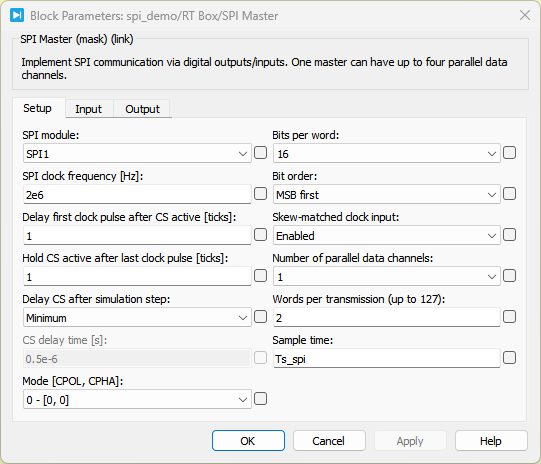
Figure 4: Block parameters of SPI Master Box
Figure 4 presents the block parameters configuration of the SPI Master block in the PLECS RT Box environment. It illustrates the key settings used to define SPI communication behavior, including the selection of SPI module, clock polarity and phase (CPOL/CPHA), number of parallel data channels, and words per transmission. The figure also highlights timing-related parameters such as chip select delay, clock delay, and SPI sample time, which control the synchronization between the RT Box simulation step and data transmission. Overall, Figure 4 presents how the SPI Master block is configured to ensure accurate, deterministic, and real-time data communication with the SPI Slave subsystem.
The SPI transmission timing can be configured to occur either within a single RT Box model step or across multiple model steps. In the single-step configuration, both the SPI transmission sample time and RT Box discretization step are equal. In the multi-step configuration, the SPI transmission sample time is larger than the RT Box discretization step, causing the communication process to span several simulation intervals.
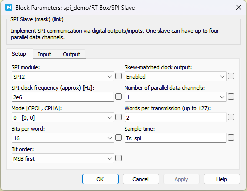
Figure 5: Block parameters of SPI Slave
Figure 5 presents the block parameter configuration of the SPI Slave in the PLECS RT Box environment. It shows the key settings required to properly synchronize the Slave operation with the SPI Master, including SPI module selection, clock polarity and phase (CPOL/CPHA), and the number of parallel data channels. The figure also highlights chip select handling, data input/output mapping, and timing configuration parameters that ensure correct sampling and interpretation of incoming SPI data. Overall, Figure 5 presents how the SPI Slave block is configured to reliably receive, decode, and respond to SPI Master transmissions in real-time operation.
The SPI communication model also includes configurable chip select delays and synchronization adjustments to emulate realistic embedded communication conditions. These features enable the system to replicate practical industrial communication interfaces used in embedded control systems.
V. Real-Time Implementation Using PLECS RT Box
The developed SPI communication model was implemented on the PLECS RT Box platform for real-time hardware-in-the-loop execution. The RT Box provides deterministic real-time simulation capabilities suitable for embedded communication validation and digital interface testing.
The real-time implementation utilizes dedicated digital input and output channels for SPI communication. The SPI clock, chip select, and data channels are physically interconnected using front-panel wiring connections. The digital outputs from the SPI Master are connected to the digital inputs of the SPI Slave, while the SPI Slave outputs are routed back toward the SPI Master receiver channels.
The real-time simulation model is compiled using the PLECS Coder and deployed directly onto the RT Box hardware. Once the model is downloaded, external mode communication enables live monitoring of the transmitted and received waveforms through the PLECS Scope interface.
The PWM synchronization signal generated within the model provides an accurate reference for evaluating timing delays and communication intervals. Oscilloscope measurements confirm correct synchronization between the PWM waveform and SPI transmission timing.
The real-time implementation demonstrates deterministic communication behavior where transmitted data accurately matches received data with predictable transmission delays. The developed framework validates the capability of the RT Box platform for embedded communication testing and industrial interface verification.
VI. SPI Communication within a Single Model Step
In the first operating scenario, the SPI communication occurs entirely within a single RT Box simulation step. The RT Box discretization step size is configured as 20 µs, while the SPI transmission sample time is also configured as 20 µs.
Under this configuration, the SPI communication process completes during every individual simulation interval. The transmitted sinusoidal, pulse, triangular, and constant signals are accurately reconstructed at the receiving subsystem without significant distortion.
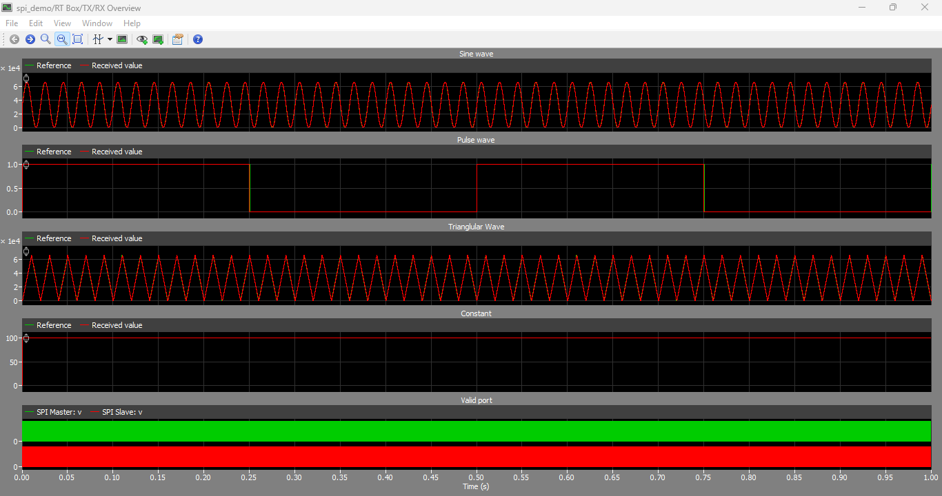
Figure 6: Transmitter and Receiver Side Waveforms which contains Sine Wave, Pulse Wave, Triagular wave, SPI Master and Slave ports signals generated by PLECS Simulation
You can download the Project files here: Download files now. (You must be logged in).
Figure 6 presents the transmitter and receiver side waveforms generated in the PLECS simulation, including the sine wave, pulse wave, triangular wave, and the corresponding SPI Master and Slave port signals. It illustrates how the original analog-like reference signals are encoded at the transmitter (SPI Master) into digital data streams and then reconstructed at the receiver (SPI Slave) with proper synchronization. The figure also highlights the timing relationship between transmitted and received signals, showing the effect of sampling and transmission delay in real-time SPI communication. Overall, Figure 6 presents the correctness and stability of bidirectional data exchange between the SPI Master and Slave subsystems in the RT Box environment.
The received waveforms exhibit staircase behavior corresponding to the discretization process of the real-time simulation. The communication delay between transmitted and received signals equals approximately two SPI transmission intervals due to the processing and synchronization mechanisms of the communication architecture.
Oscilloscope measurements demonstrate that the SPI clock pulses, chip select signals, and digital data transmission occur entirely within one simulation period. The synchronized PWM signal confirms accurate timing alignment between communication events and RT Box execution intervals.
This operating mode is suitable for applications requiring fast communication updates and deterministic timing performance. The results confirm stable communication behavior and reliable data transfer within real-time simulation constraints.
VII. SPI Communication over Multiple Model Steps
The second operating scenario investigates SPI communication extending over multiple RT Box simulation steps. In this configuration, the RT Box discretization step size is reduced to 5 µs while the SPI transmission sample time remains 20 µs.
Because the communication interval exceeds the simulation step size, the SPI transmission process spans four separate RT Box execution periods. The received waveforms continue to match the transmitted signals; however, the incoming data updates occur at a slower interval corresponding to the SPI sample time.
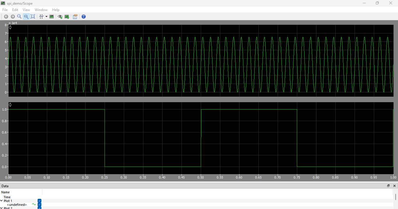
Figure 7: SPI waveforms of Sine and Square wave
Figure 7 presents the SPI waveforms corresponding to the transmission and reception of sine and square (pulse) signals in the PLECS RT Box simulation. It illustrates how the SPI Master encodes these input waveforms into digital data packets and transmits them through the SPI clocked communication interface. On the receiver side, the SPI Slave reconstructs the incoming data to reproduce the original sine and square waveforms with proper synchronization. The figure also highlights the discrete nature of SPI sampling, where the continuous reference signals are updated at specific transmission intervals defined by the SPI sample time. Overall, Figure 7 presents the accurate digital representation and successful reconstruction of sine and square waveforms through real-time SPI communication.
The staircase resolution of the reference waveform becomes finer due to the smaller discretization step size. Meanwhile, the received SPI data maintains its update interval according to the communication timing configuration.
Oscilloscope measurements verify that the SPI communication occupies four complete simulation intervals. The synchronized PWM waveform confirms the exact relationship between the RT Box model step size and SPI transmission duration.
This operating mode demonstrates the flexibility of the RT Box SPI interface for handling communication systems requiring transmission intervals longer than the simulation step size. The results confirm stable operation and accurate synchronization under multi-step communication conditions.
VIII. External ADC Interface Demonstration
An advanced implementation of the SPI communication architecture was developed using an external analog-to-digital converter (ADC) evaluation board connected to the RT Box. In this configuration, the RT Box functions as the SPI Master while the ADC board acts as the SPI Slave.
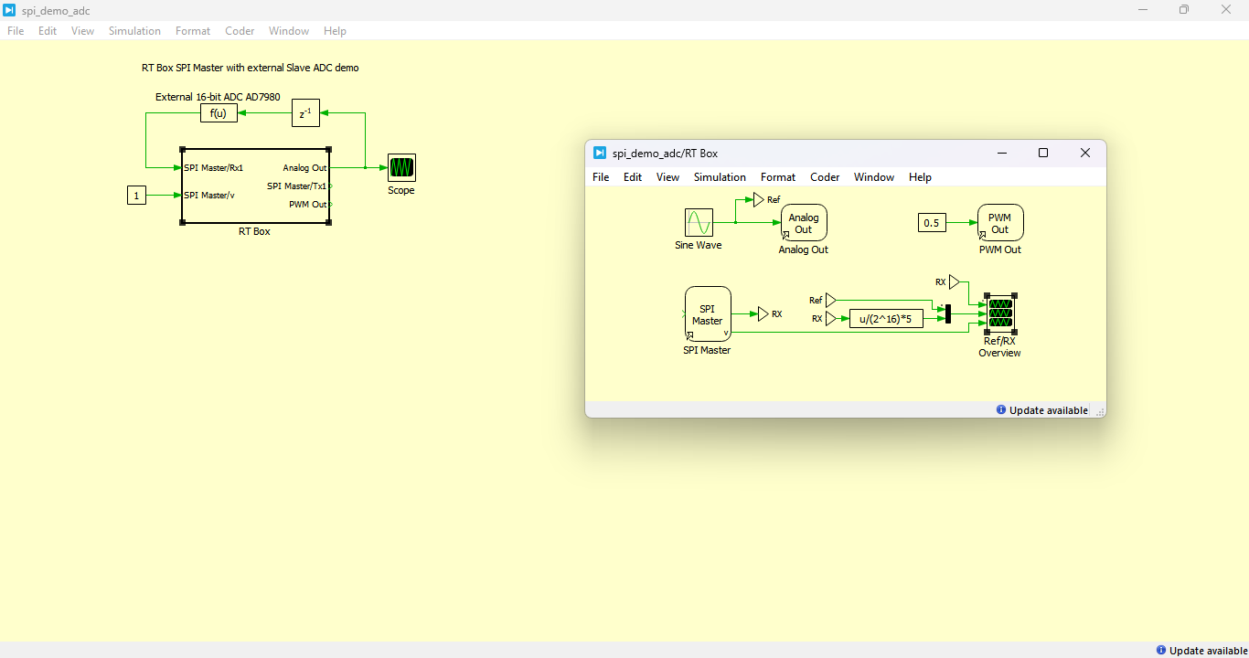
Figure 8: SPI Master and Slave configuration circuit with ADC schematics in PLECS Simulation
You can download the Project files here: Download files now. (You must be logged in).
Figure 8 presents the SPI Master and Slave configuration circuit integrated with an external ADC schematic in the PLECS simulation environment. It illustrates how the SPI Master generates control signals such as clock and chip select while transmitting reference analog signals converted into digital data for communication with the SPI Slave. The figure also shows the ADC interface, where an analog input signal is sampled and converted into a 16-bit digital representation before being transmitted through the SPI protocol. On the receiving side, the SPI Slave processes the incoming digital data and reconstructs the corresponding signal for further analysis. Overall, Figure 8 presents the complete SPI-based data acquisition system, combining ADC conversion and SPI communication within the RT Box platform for real-time embedded simulation.
The RT Box generates a sinusoidal analog signal ranging between 0.5 V and 4.5 V. The external ADC converts this analog signal into 16-bit digital data which is transmitted back to the RT Box through the SPI communication interface.
The received digital data is reconstructed into an equivalent analog waveform for comparison with the original reference signal. Experimental results confirm accurate signal conversion and successful SPI communication between the RT Box and the external ADC hardware.
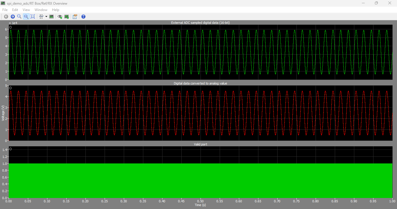
Figure 9: External ADC Sampled Digital data, analog data value and port communications waveforms
Figure 9 presents the external ADC sampled digital data, reconstructed analog data values, and corresponding port communication waveforms obtained from the PLECS RT Box simulation. It illustrates how the analog input signal is first sampled by the external ADC and converted into a 16-bit digital representation, which is then transmitted through the SPI communication interface. The SPI port signals, including clock, chip select, and data lines, are also shown to highlight the synchronization between data conversion and transmission. On the receiving side, the digital data is converted back into an equivalent analog value for comparison with the original reference signal. Overall, Figure 9 presents the complete interaction between analog signal acquisition, SPI-based digital transmission, and reconstructed analog output in a real-time simulation environment.
This advanced demonstration validates the capability of the developed architecture for real embedded communication systems involving external sensors, converters, and industrial devices.
IX. Results and Discussion
The real-time simulation results confirm successful implementation of SPI communication using the PLECS RT Box platform. The transmitted and received waveforms demonstrate accurate bidirectional data transfer between the SPI Master and SPI Slave subsystems.
The sinusoidal, pulse, triangular, and constant signals are correctly reconstructed after transmission through the SPI interface. The received signals closely match the original transmitted signals in terms of amplitude, waveform shape, and frequency characteristics. This validates the correctness of the SPI communication protocol implementation.
The single-step communication mode demonstrates high-speed deterministic communication where SPI transmission occurs entirely within one RT Box simulation step. Oscilloscope measurements confirm synchronization between the PWM timing signal and SPI communication intervals.
The multi-step communication mode successfully demonstrates communication spanning multiple simulation intervals. The results verify that the SPI interface remains stable and synchronized even when the communication duration exceeds the RT Box discretization step size.
The external ADC demonstration further validates the practical applicability of the developed framework for embedded systems and industrial communication applications. Accurate analog-to-digital conversion and successful SPI transmission confirm compatibility with external hardware peripherals.
The developed architecture provides a highly flexible platform for embedded communication analysis, hardware-in-the-loop validation, and industrial digital interface testing. The modular structure allows future integration with advanced embedded controllers, distributed communication systems, and industrial automation platforms.
X. Conclusion
This paper presented the development and real-time implementation of an SPI communication interface using the PLECS RT Box platform. The proposed architecture successfully demonstrated bidirectional SPI communication between SPI Master and SPI Slave subsystems implemented within a real-time hardware-in-the-loop environment.
The developed model validated both single-step and multi-step SPI transmission scenarios using synchronized PWM timing analysis and oscilloscope measurements. The results confirmed accurate communication timing, reliable data transfer, deterministic synchronization, and stable real-time operation.
The implementation additionally demonstrated integration with an external ADC evaluation board, highlighting the suitability of the developed framework for practical embedded systems and industrial communication applications.
The developed SPI communication architecture provides an effective platform for testing embedded digital interfaces, validating communication protocols, and studying real-time synchronization behavior in industrial automation systems. Future work may include implementation of advanced communication protocols, multi-device SPI networks, FPGA-based communication acceleration, and integration with real industrial embedded controllers.
References
[1] Plexim GmbH, SPI Interface Demo on a Single RT Box, RT Box Target Support Package 2.2.1, Switzerland, 2023.
[2] J. Allmeling and N. Felderer, “Real-Time Simulation Techniques for Embedded Systems and Power Electronics,” IEEE Industrial Electronics Conference, 2017.
[3] Texas Instruments, SPI Communication Protocol Reference Guide, Texas Instruments Incorporated, 2022.
[4] Analog Devices, AD7980 16-Bit Analog-to-Digital Converter Datasheet, Analog Devices Inc., 2021.
[5] Plexim GmbH, PLECS RT Box User Manual, Switzerland, 2023.
You can download the Project files here: Download files now. (You must be logged in).


Responses