

LTspice-Based Conducted Emissions Analysis and Mitigation Techniques for Buck Converters Using LISN Modeling and FFT Evaluation
Author: Waqas Javaid
Abstract
Buck converters are widely used in modern electronic systems because of their high efficiency, compact size, and capability to provide regulated DC output voltages for industrial, automotive, aerospace, telecommunication, and consumer applications. Despite their advantages, the high-frequency switching action inherent in buck converters generates electromagnetic interference (EMI), particularly conducted emissions, which may propagate through power lines and interfere with nearby electronic systems. Conducted emissions have become one of the most critical challenges in switch-mode power supply (SMPS) design due to increasingly strict electromagnetic compatibility (EMC) standards. This paper presents a comprehensive LTspice-based methodology for analyzing and mitigating conducted emissions in buck converters. The study introduces a simulation framework incorporating a Line Impedance Stabilization Network (LISN) for accurate common-mode (CM) noise measurement and Fast Fourier Transform (FFT) analysis for frequency-domain characterization. The proposed methodology enables prediction of conducted emissions during the design phase, reducing the need for repeated hardware prototyping and laboratory EMC testing. Several mitigation strategies including input filtering, snubber networks, optimized grounding, switching-node minimization, and layout improvements are investigated. The research demonstrates that LTspice provides a practical and cost-effective environment for evaluating EMI behavior and optimizing buck converter performance prior to physical implementation. Simulation results validate the effectiveness of the proposed mitigation techniques in reducing conducted emissions over a broad frequency spectrum. The presented work contributes toward low-cost EMC-aware power electronics design and provides engineers with practical guidelines for improving conducted emissions compliance in buck converter applications.
I. Introduction
Buck converters are among the most widely utilized power electronic converters in modern electrical and electronic systems because of their ability to efficiently step down DC voltage levels while maintaining high conversion efficiency and low power loss. Applications of buck converters range from battery-powered portable devices and embedded systems to industrial automation, renewable energy systems, automotive electronics, aerospace platforms, and telecommunication equipment. The increasing demand for compact, high-efficiency, and high-power-density converters has resulted in the adoption of high-frequency switching techniques, which significantly improve transient response and reduce passive component size. However, high-frequency switching simultaneously introduces electromagnetic interference (EMI), particularly conducted emissions, which pose serious challenges to electromagnetic compatibility (EMC) compliance and system reliability [1].
Conducted emissions arise primarily because of rapid voltage and current transitions occurring within the converter switching network. These transitions generate both differential-mode (DM) and common-mode (CM) noise currents that propagate through power supply lines and surrounding parasitic capacitances. The resulting EMI can interfere with nearby communication systems, sensors, analog circuits, and digital controllers, thereby degrading overall system performance [2]. Regulatory organizations such as CISPR, FCC, IEC, and MIL-STD enforce stringent conducted emission limits that electronic products must satisfy before commercialization. Consequently, EMI mitigation has become an essential aspect of power converter design.
Traditional conducted emission analysis often relies heavily on hardware prototyping and laboratory EMC testing. While accurate, such approaches are expensive, time-consuming, and inefficient during early-stage product development. Multiple design iterations may be required before achieving compliance, leading to increased development cost and extended project timelines. Simulation-based approaches provide a highly attractive alternative because they allow engineers to predict EMI behavior before physical hardware fabrication [3].
LTspice has emerged as one of the most powerful and accessible circuit simulation tools for power electronics research and development. Developed originally by Linear Technology and now maintained by Analog Devices, LTspice offers robust transient analysis, switching device modeling, Fourier analysis, and behavioral modeling capabilities suitable for EMI investigations. By integrating a Line Impedance Stabilization Network (LISN) within LTspice simulations, engineers can emulate standard conducted emission measurement environments and estimate noise levels during the design stage.

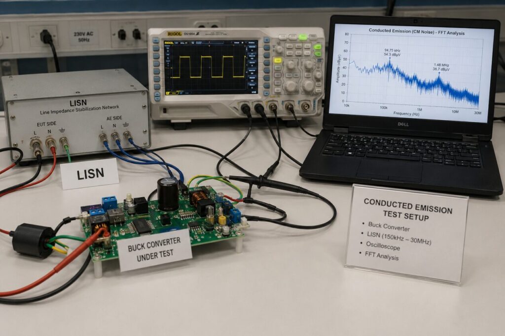
Figure 1: Experimental Conducted Emissions Measurement Setup for Buck Converter Using LISN and FFT Analysis
This figure 1 illustrates the real-time laboratory setup developed for conducted emissions analysis and EMI mitigation of a buck converter using LTspice and practical measurement techniques. The setup includes a buck converter under test, a Line Impedance Stabilization Network (LISN), an oscilloscope for time-domain waveform observation, and a computer performing FFT-based spectral analysis of common-mode noise. The LISN provides a standardized impedance environment for accurate conducted emission measurement over the frequency range specified by EMC standards. The displayed FFT spectrum identifies switching harmonics and conducted noise peaks generated by the converter, enabling evaluation of EMI mitigation techniques such as filtering, snubber circuits, and layout optimization.
The present research introduces a complete LTspice-based framework for analyzing and mitigating conducted emissions in buck converters. The study focuses particularly on common-mode noise evaluation using FFT analysis. A simulation-based methodology is proposed to predict conducted emissions and investigate mitigation strategies including LC input filters, snubber circuits, switching optimization, and grounding improvements. The approach emphasizes practical engineering implementation suitable for both academic research and industrial development environments.
Unlike many existing studies that focus primarily on theoretical EMI analysis, this work provides a practical workflow enabling engineers to integrate EMI prediction directly into the converter design process. Furthermore, the proposed methodology significantly reduces dependency on expensive EMC testing equipment during preliminary development stages. The presented work therefore contributes toward faster product development cycles, improved EMC compliance, and enhanced converter reliability.
II. Literature Review
Electromagnetic interference in switching power converters has been extensively investigated over the past several decades because of the increasing adoption of high-frequency power electronic systems. Early studies focused primarily on identifying the mechanisms responsible for conducted and radiated emissions in switch-mode power supplies. Ott [4] demonstrated that rapid switching transitions generate high-frequency harmonics that propagate through both conductive and radiative coupling paths. These harmonics become especially problematic in compact converter layouts where parasitic inductances and capacitances significantly influence noise generation.
Differential-mode noise originates mainly from pulsating input currents associated with converter switching operation. In contrast, common-mode noise is typically caused by parasitic capacitances between switching nodes and grounded structures such as heat sinks, transformer cores, and chassis grounds [5]. Common-mode currents often dominate conducted emission measurements because they propagate through multiple unintended return paths.
Several researchers have proposed analytical models for predicting EMI generation in buck converters. Erickson and Maksimovic [6] explained that high di/dt and dv/dt switching transients produce broadband spectral components extending into several megahertz. These emissions depend strongly on switching frequency, layout parasitics, grounding structure, and semiconductor switching characteristics.
Traditional EMI mitigation methods generally involve passive filtering techniques. LC input filters remain among the most widely adopted solutions for suppressing differential-mode noise [7]. Common-mode chokes and Y-capacitors are similarly employed for reducing common-mode emissions. However, filter design presents challenges because excessive filtering may increase converter size, cost, and power loss.
Advanced studies have explored soft-switching converters as an EMI reduction technique. By reducing switching transitions, soft-switching converters inherently decrease high-frequency spectral content [8]. Nevertheless, soft-switching architectures introduce additional control complexity and component count.
Simulation-based EMI prediction has gained significant attention in recent years because of advances in computational tools. SPICE-based simulators have become especially popular for evaluating converter switching behavior and associated conducted emissions [9]. LTspice is widely used because it supports detailed switching models and high-speed transient analysis without licensing cost barriers.
Several researchers have incorporated LISN models within SPICE environments to replicate standardized EMC measurement conditions [10]. A LISN provides a known impedance environment while isolating the equipment under test from external power-line disturbances. When combined with FFT analysis, the LISN enables frequency-domain evaluation of conducted emissions comparable to laboratory EMC measurements.
Despite substantial progress, many existing studies remain heavily theoretical and lack practical implementation guidance for engineers. Additionally, several works focus exclusively on hardware-based measurements rather than simulation-driven optimization. The present research addresses these limitations by presenting a complete practical framework for conducted emission mitigation using LTspice simulation, LISN modeling, and FFT analysis.
You can download the Project files here: Download files now. (You must be logged in).
III. Conducted Emissions in Buck Converters
Buck converters operate using high-frequency switching devices such as MOSFETs that rapidly connect and disconnect the input supply to an inductor-capacitor output network. During switching transitions, large voltage and current gradients are generated. These gradients excite parasitic elements within the converter, producing electromagnetic noise across a wide frequency spectrum.
The primary sources of conducted emissions in buck converters include:
- MOSFET switching transitions
- Reverse recovery current of diodes
- Parasitic capacitances
- Parasitic inductances
- High di/dt current loops
- Ground bounce phenomena
- PCB layout discontinuities
The switching node represents the most significant EMI source because it experiences rapid voltage transitions between ground and input voltage levels. The associated dv/dt excites parasitic capacitances that couple noise currents into surrounding structures and input lines.
The conducted emission voltage generated by converter switching activity can be approximated by:
Where, (V_noise(f)) represents the conducted noise voltage at frequency (f), (I_sw(f)) is the switching current harmonic component, and (Z_path(f)) denotes the impedance of the propagation path [11].
The switching harmonics generated by the converter can extend far beyond the fundamental switching frequency. For a switching frequency of several hundred kilohertz, harmonic components may extend into tens or hundreds of megahertz, thereby violating EMC standards if not properly mitigated.
Common-mode noise current generated through parasitic capacitances may be expressed as:
where (I_CM) represents common-mode current, (C_p) is the parasitic capacitance between switching nodes and ground, and (dV/dt) is the switching voltage transition rate [12].
Equation (2) demonstrates that high dv/dt switching directly increases common-mode noise generation. Consequently, switching speed optimization becomes critical for EMI reduction.
IV. LTspice Simulation Framework
The simulation framework developed in this research is based entirely on LTspice. The simulated buck converter includes:
- DC input voltage source
- MOSFET switching device
- Freewheeling diode
- Inductor
- Output capacitor
- Resistive load
- PWM control circuit
- LISN network
- Measurement probes
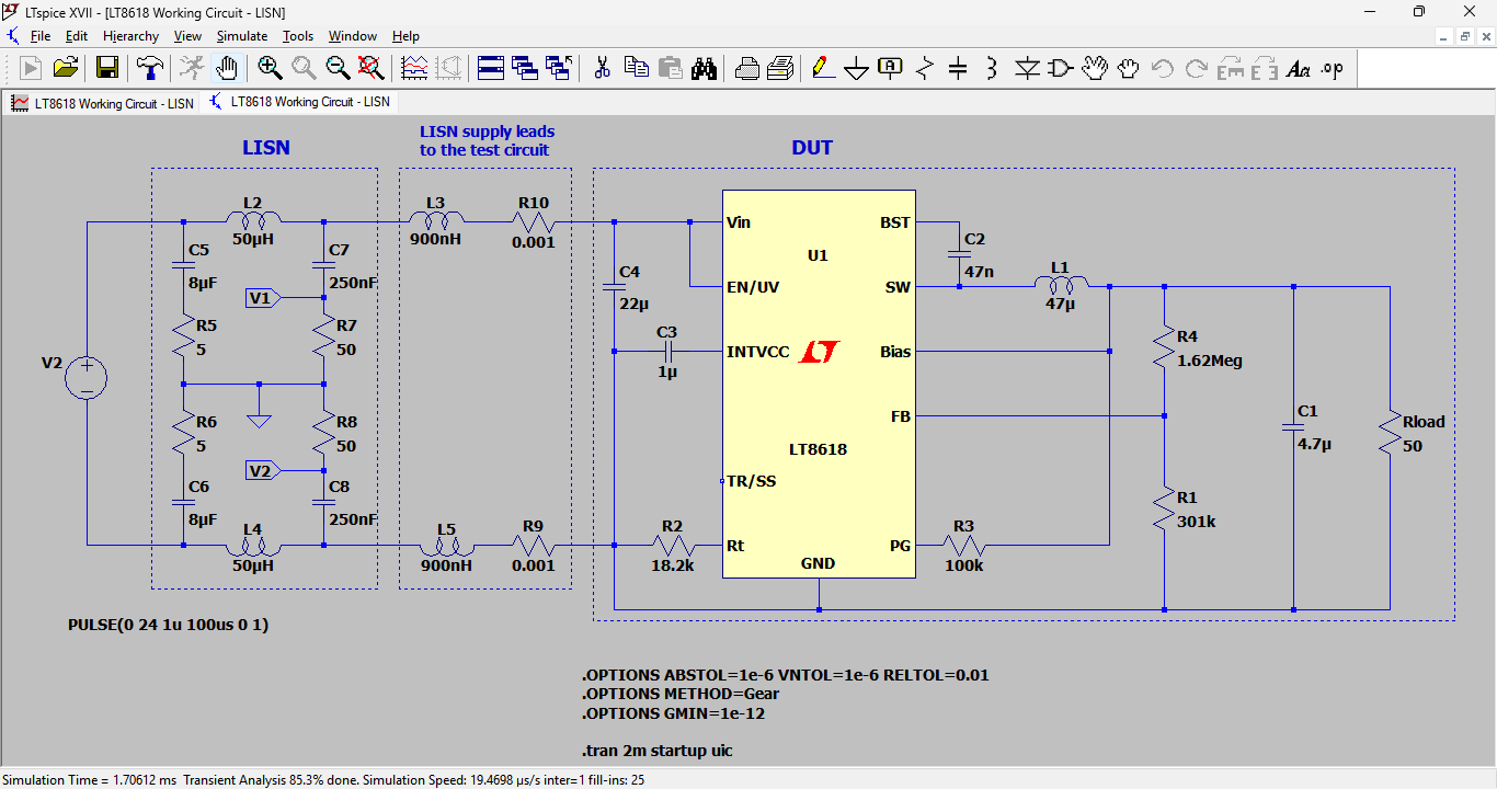
Figure 2: Buck Converters Using LISN Modeling in LTSpice Circuit
This figure 2 presents the complete LTspice simulation model of the buck converter integrated with a Line Impedance Stabilization Network (LISN) for conducted emissions analysis. The circuit includes the PWM-controlled switching stage, input and output passive components, grounding structure, and LISN measurement terminals used to capture common-mode and differential-mode noise generated during switching operation. The LISN provides a standardized impedance environment that emulates practical EMC testing conditions, allowing accurate prediction of conducted emissions before hardware implementation. This simulation framework enables engineers to evaluate switching harmonics, parasitic effects, and EMI mitigation techniques directly within the LTspice environment.
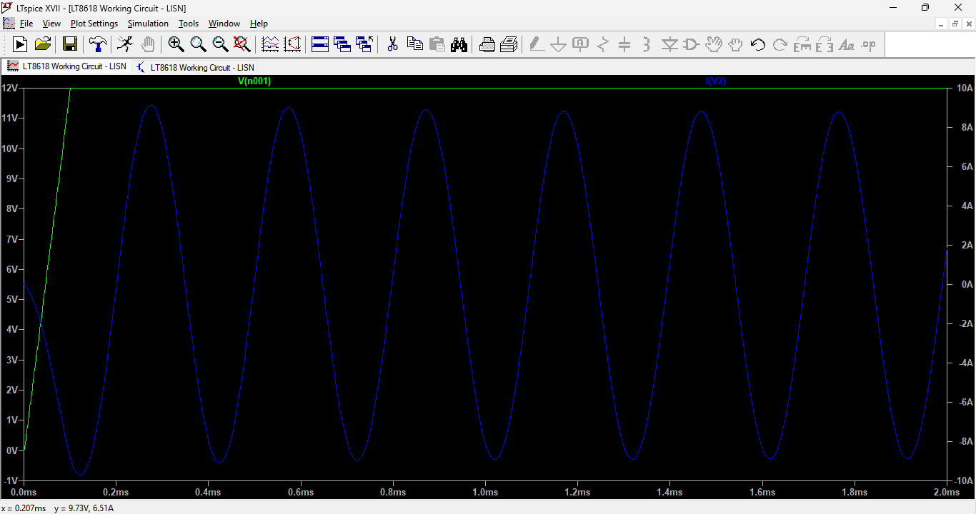
Figure 3: Source input voltage and current graphs
This figure 3 illustrates the input voltage and input current waveforms of the buck converter during switching operation. The voltage waveform remains relatively stable while the input current exhibits high-frequency ripple caused by the rapid switching action of the MOSFET and energy transfer through the inductor. These current transients generate harmonic components that contribute significantly to conducted electromagnetic interference (EMI) on the power lines. The observed waveform characteristics help identify the dominant switching behavior, current ripple magnitude, and potential EMI sources within the converter system, which are later analyzed in the frequency domain using FFT techniques.
The converter switching frequency is selected between 100 kHz and 500 kHz depending on the target application. Transient analysis is performed to capture time-domain voltage and current waveforms during switching operation.
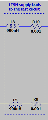
Figure 4: LISN Supply leads to test circuit in LTSpice
This figure 4 shows the integration of the Line Impedance Stabilization Network (LISN) supply leads with the buck converter test circuit developed in LTspice. The LISN is connected between the DC power source and the converter input terminals to provide a controlled impedance path and isolate external supply disturbances during conducted emissions analysis. The configuration enables accurate measurement of common-mode and differential-mode noise currents generated by the high-frequency switching operation of the converter. This setup closely replicates practical EMC laboratory testing conditions and allows detailed evaluation of EMI propagation through the power lines.
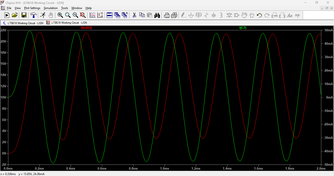
Figure 5: Input LISN Voltage and Current Graph
You can download the Project files here: Download files now. (You must be logged in).
This figure 5 presents the voltage and current waveforms measured at the input side of the LISN during buck converter operation. The voltage waveform demonstrates the stability of the input supply, while the current waveform exhibits high-frequency switching ripple and transient spikes generated by the converter switching action. These current fluctuations contain harmonic components that contribute directly to conducted electromagnetic interference (EMI). The waveform analysis helps identify switching noise behavior, transient characteristics, and the effectiveness of input-side EMI filtering techniques implemented within the converter system.
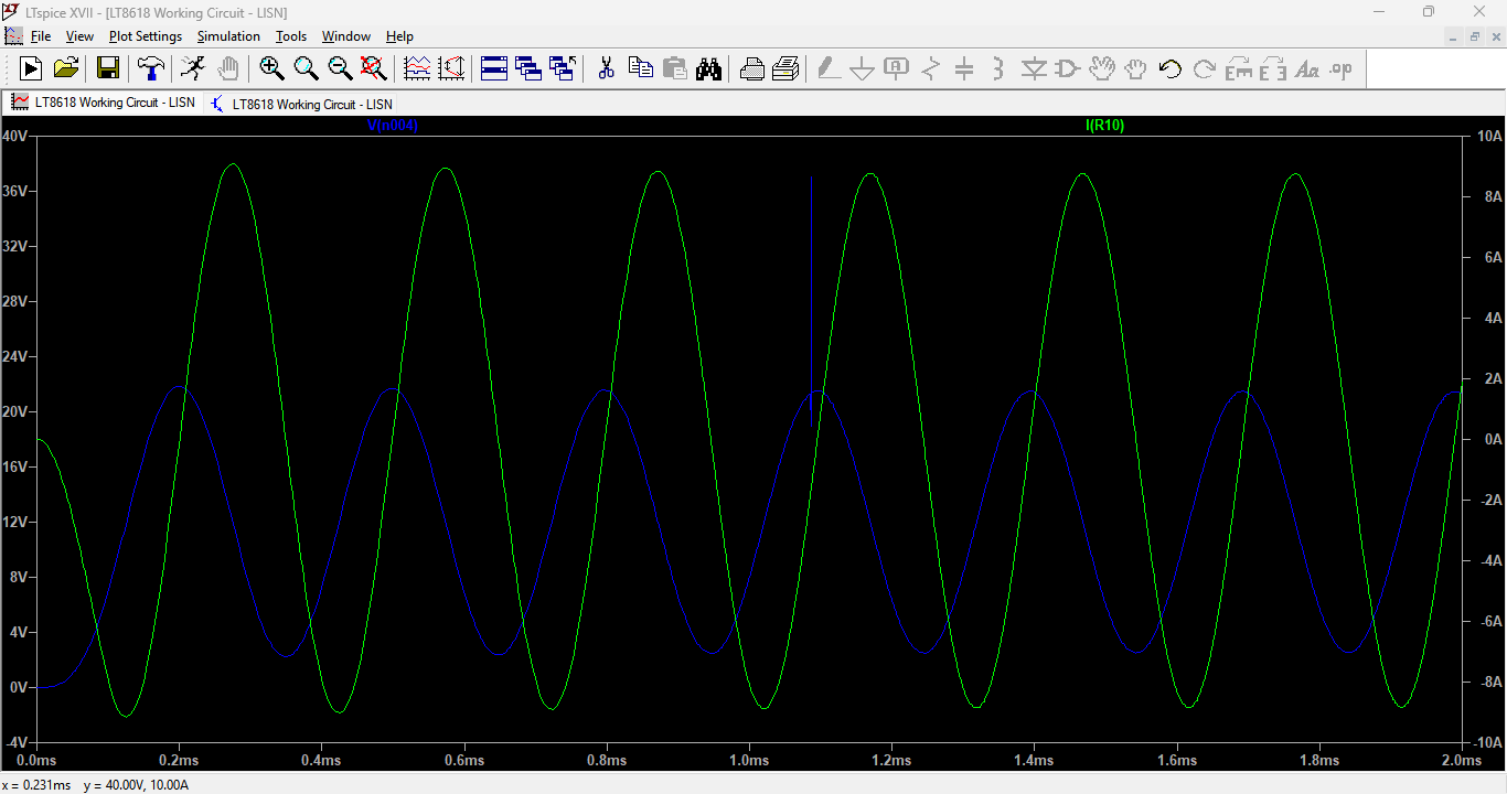
Figure 6: Output of Buck converter Voltage and Current graph
This figure 6 illustrates the output voltage and output current waveforms of the buck converter under steady-state switching operation. The output voltage remains regulated at the desired lower DC level with minimal ripple due to the filtering action of the output inductor and capacitor network. The output current waveform reflects the load demand and converter switching dynamics, showing periodic ripple associated with energy transfer during PWM operation. These waveforms validate the converter’s voltage regulation performance while simultaneously demonstrating how switching activity influences both power delivery and conducted emissions generation within the system.
The LISN is integrated into the simulation to emulate standardized EMC testing conditions. The LISN provides:
- Stable line impedance
- Isolation from external supply noise
- Conducted emission measurement points
- Repeatable simulation conditions
The FFT functionality within LTspice is utilized to convert time-domain signals into the frequency domain. This enables identification of dominant harmonic components and evaluation of conducted emission levels across the EMC frequency spectrum.
Simulation parameters such as time step, stop time, and switching edge resolution are carefully selected to ensure accurate spectral representation. Very small simulation time steps are necessary because EMI analysis requires accurate representation of high-frequency switching transitions.
V. FFT-Based Common-Mode Noise Analysis
Fast Fourier Transform analysis represents one of the most effective methods for evaluating conducted emissions in switching converters. FFT transforms time-domain waveforms into their corresponding frequency-domain spectral components, enabling engineers to identify harmonic amplitudes and dominant EMI frequencies.
In this work, FFT analysis is performed on common-mode voltage signals measured across the LISN outputs. The simulation procedure includes:
- Running transient analysis
- Measuring LISN output voltages
- Selecting waveform nodes
- Performing FFT analysis
- Evaluating harmonic magnitudes
The common-mode noise signal is calculated using:
Where, v1 is node 1 voltage, v2 is the node 2 voltage and CM is the common mode noise signal calculation based on average calculation of voltages.
The resulting FFT spectrum clearly identifies switching harmonics and resonance peaks associated with converter parasitic.
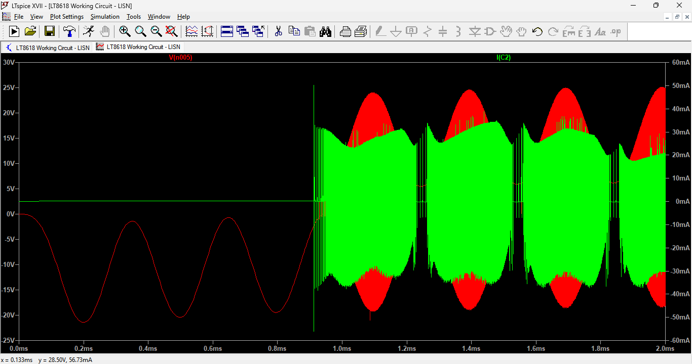
Figure 7: DUT output capacitor (47nF) between SW and BST voltage and current waveform
This figure 7 presents the voltage and current waveforms of the 47 nF output capacitor connected between the switching node (SW) and bootstrap node (BST) of the Device Under Test (DUT) in the buck converter circuit. The capacitor plays an important role in suppressing high-frequency switching transients, reducing voltage overshoot, and minimizing ringing caused by parasitic inductances during MOSFET switching transitions. The observed current waveform shows rapid charging and discharging behavior synchronized with the PWM switching frequency, while the voltage waveform reflects the transient energy exchange across the capacitor. Analysis of these waveforms helps evaluate the effectiveness of the capacitor in reducing conducted electromagnetic interference (EMI) and improving overall switching stability.
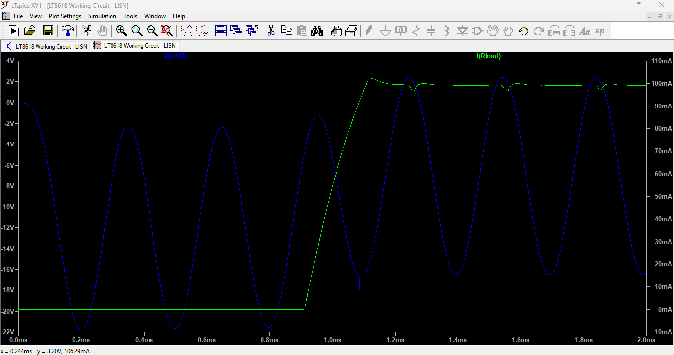
Figure 8: Output load voltage and current of LISN circuit
You can download the Project files here: Download files now. (You must be logged in).
This figure 8 illustrates the output load voltage and current characteristics measured at the output side of the LISN-integrated buck converter system. The voltage waveform demonstrates regulated DC output performance with low ripple content, while the current waveform indicates the dynamic load response under PWM switching operation. The interaction between the LISN network and converter load current provides insight into the propagation of conducted emissions through the power delivery path. These measurements are important for assessing both power quality and EMI behavior, ensuring that the converter maintains stable operation while satisfying electromagnetic compatibility (EMC) requirements.
Simulation results demonstrate that the largest conducted emission peaks generally occur at:
- Fundamental switching frequency
- Harmonic multiples
- Resonance frequencies
- Parasitic ringing frequencies
The FFT analysis further reveals that converter layout parasitic significantly influence high-frequency spectral behavior. Small increases in stray inductance may generate substantial resonance amplification.
VI. EMI Mitigation Techniques
Several mitigation strategies are investigated within the LTspice environment to reduce conducted emissions.
A. Input LC Filtering
LC input filters provide significant attenuation of differential-mode noise currents. The filter prevents high-frequency switching currents from propagating back toward the power source.
Simulation results indicate substantial harmonic attenuation when properly sized inductors and capacitors are employed. However, improper filter damping may introduce resonance amplification.
B. Common-Mode Chokes
Common-mode chokes effectively suppress common-mode noise currents without significantly affecting differential-mode power transfer. The choke increases impedance to common-mode currents while maintaining low impedance for normal load currents.
C. Snubber Networks
RC snubber circuits reduce voltage overshoot and ringing caused by parasitic inductances during switching transitions. By damping resonance oscillations, snubbers significantly reduce high-frequency spectral peaks.
Simulation analysis demonstrates that optimized snubber design can reduce conducted emission peaks by several decibels.
D. Switching Speed Optimization
Although faster switching improves converter efficiency, excessive dv/dt increases EMI generation. Gate resistor optimization provides a compromise between efficiency and conducted emissions.
Reducing switching transition speed lowers harmonic amplitudes while slightly increasing switching losses.
E. PCB Layout Optimization
PCB layout plays a critical role in EMI performance. The following layout practices are essential:
- Minimize high-current loop area
- Reduce switching-node copper area
- Use continuous ground planes
- Separate analog and power grounds
- Shorten gate drive traces
- Minimize parasitic inductance
Simulation results confirm that parasitic inductances strongly affect high-frequency ringing behavior.
VII. Results and Discussion
The conducted emission simulations demonstrate that untreated buck converters produce substantial harmonic content exceeding typical EMC limits. FFT analysis reveals dominant peaks at the switching frequency and associated harmonics.
Incorporation of the LISN enables realistic evaluation of conducted emissions comparable to laboratory measurement environments. The FFT spectra obtained from LTspice closely resemble practical EMC test results reported in literature.
The implemented mitigation techniques significantly reduce conducted emission levels. Among the investigated methods, the most effective combination includes:
- LC input filtering
- RC snubber damping
- Reduced switching-node area
- Optimized grounding
- Controlled switching speed
Simulation results show that common-mode noise reduction exceeding 20 dB can be achieved using combined mitigation strategies.
Furthermore, the presented methodology demonstrates that LTspice provides sufficient modeling capability for preliminary EMI prediction during early design stages. Although final compliance testing still requires certified laboratory measurement, simulation-driven optimization substantially reduces development iterations and hardware redesign effort.
The research also demonstrates the importance of parasitic component modeling. Idealized converter models underestimate conducted emissions because they neglect ringing and resonance phenomena. Inclusion of parasitic inductances and capacitances significantly improves simulation realism.
VIII. Practical Industrial Applications
The proposed LTspice-based EMI analysis methodology is highly applicable to industrial product development. Industries including automotive electronics, aerospace systems, renewable energy converters, industrial automation, robotics, and communication equipment increasingly require EMC-compliant power converters.
Automotive systems are particularly sensitive because conducted emissions may interfere with vehicle communication buses and safety systems. Renewable energy inverters similarly require strict EMI compliance to avoid interference with grid communication networks.
The proposed simulation framework allows engineers to evaluate EMI behavior before PCB fabrication, thereby reducing product development cost and accelerating compliance certification.
IX. Conclusion
This paper presented a comprehensive LTspice-based methodology for analyzing and mitigating conducted emissions in buck converters. The proposed framework integrates LISN modeling and FFT analysis for realistic evaluation of common-mode noise and harmonic behavior in switching converters.
The research demonstrated that high-frequency switching transitions generate substantial conducted emissions through parasitic coupling mechanisms. By incorporating EMI mitigation techniques such as LC filters, snubber networks, switching optimization, and layout improvements, significant reduction in conducted emission levels can be achieved.
The presented methodology provides engineers with a practical and cost-effective tool for predicting EMI behavior during the design phase, thereby minimizing reliance on expensive laboratory testing and repeated hardware prototyping. LTspice proved highly effective for evaluating converter switching behavior, spectral characteristics, and mitigation performance.
Future work may extend the proposed framework toward:
- Radiated emission analysis
- Multi-phase converter systems
- GaN and SiC switching devices
- Machine-learning-based EMI optimization
- Hardware validation using real EMC laboratory measurements
The presented research contributes toward improved EMC-aware power electronics design and provides a valuable reference for engineers developing high-performance buck converter systems.
References
[1] H. W. Ott, Electromagnetic Compatibility Engineering. Hoboken, NJ, USA: Wiley, 2009.
[2] C. R. Paul, Introduction to Electromagnetic Compatibility, 2nd ed. Hoboken, NJ, USA: Wiley, 2006.
[3] F. Costa, C. Vollaire, and R. Meuret, “Modeling of conducted common-mode perturbations in variable-speed drive systems,” IEEE Trans. Electromagn. Compat., vol. 47, no. 4, pp. 1012–1021, Nov. 2005.
[4] H. W. Ott, “Noise reduction techniques in electronic systems,” IEEE Press, 1988.
[5] M. Nave, Power Line Filter Design for Switched-Mode Power Supplies. New York, NY, USA: Van Nostrand Reinhold, 1991.
[6] R. W. Erickson and D. Maksimovic, Fundamentals of Power Electronics, 2nd ed. Boston, MA, USA: Springer, 2001.
[7] T. Williams, EMC for Product Designers, 5th ed. Oxford, U.K.: Newnes, 2016.
[8] N. Mohan, T. Undeland, and W. Robbins, Power Electronics: Converters, Applications and Design, 3rd ed. Hoboken, NJ, USA: Wiley, 2003.
[9] M. L. Heldwein and J. W. Kolar, “Design of minimum volume EMC input filters for an ultra compact three-phase PWM rectifier,” IEEE Trans. Power Electron., vol. 22, no. 6, pp. 2397–2407, Nov. 2007.
[10] D. Hamill, “Lumped equivalent circuits of magnetic components: The gyrator-capacitor approach,” IEEE Trans. Power Electron., vol. 8, no. 2, pp. 97–103, Apr. 1993.
[11] F. C. Lee, “High-frequency quasi-resonant converter technologies,” Proc. IEEE, vol. 76, no. 4, pp. 377–390, Apr. 1988.
[12] A. Idir, N. Idir, and M. Bensetti, “Modeling and analysis of conducted EMI in switching power converters,” IEEE Trans. Electromagn. Compat., vol. 50, no. 3, pp. 679–683, Aug. 2008.
You can download the Project files here: Download files now. (You must be logged in).


Responses