

Design and Execution of a Logisim 4-Bit Arithmetic Logic Unit (ALU) with Overflow and Zero Flags

Author: Waqas Javaid
Abstract
The design, implementation, and verification of a 4-bit Arithmetic Logic Unit (ALU) utilizing Logisim simulation software are presented in this work. Eight operations—Increment, Addition, Decrement, Subtraction, NOT, OR, AND, and XOR—are supported by the ALU and can be chosen via a 3-bit control bus (S2, S1, S0). By enclosing the ALU as a reusable logical block, the architecture adheres to modular hierarchical concepts. Two 4-bit operand inputs (A, B), one 4-bit result output (S), and two status flags (Overflow (OF) and Zero (ZF)) are all present in the circuit. Logic tables, binary examples, and gate-level implementations are used to analyze each operation. As a sample bitwise function, the OR operation is thoroughly analyzed. All selection codes are verified and the ALU is checked using Logisim’s iterative input techniques. The outcomes validate timing-independent digital logic performance, flag activation, and proper functional behavior.
Introduction
The Arithmetic Logic Unit (ALU) is a fundamental component of any central processing unit (CPU). It performs arithmetic (e.g., addition, subtraction) and logical (e.g., AND, OR, XOR) operations on binary numbers. In modern digital design, ALUs are often simulated before hardware implementation to verify correctness, reduce errors, and optimize resource usage [1].
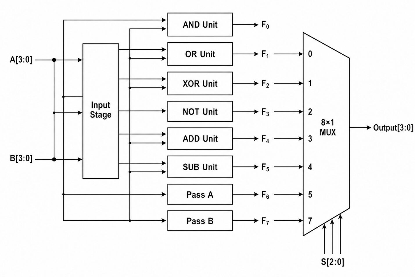
Figure 1: Block diagram of 4-bit ALU including input stage, logical operations, MUX (8×1) and output stage
This figure 1 shows a 4-bit Arithmetic Logic Unit (ALU) where two inputs A[3:0]A[3:0]A[3:0] and B[3:0]B[3:0]B[3:0] are fed into an input stage and processed by multiple functional units. The ALU performs logical (AND, OR, XOR, NOT), arithmetic (ADD, SUB), and data transfer (Pass A, Pass B) operations simultaneously. An 8×1 multiplexer selects one of these operation results using control signals S[2:0]S[2:0]S[2:0] to produce the final 4-bit output. This report details the complete design process of a 4-bit ALU using Logisim, a popular educational logic simulation tool [2]. The ALU accepts two 4-bit inputs (A and B), a 3-bit selection code (S2, S1, S0), and produces a 4-bit result (S) along with two flags: Overflow (OF) for signed arithmetic overflow and Zero (ZF) indicating a zero result. Eight operations are implemented, as shown in Table 2.
The objectives of this work are:
- To create a modular, reusable ALU block in Logisim.
- To use iterative test elements (input pins, selection controls, output displays) for exhaustive verification.
- To document all inputs, outputs, and internal logic with clear nomenclature.
- To produce binary and logic tables for each operation, with special attention to the OR operation.
- To present the design in a format suitable for an IEEE-style research paper.
The remainder of this paper is organized as follows: Section 2 describes the ALU architecture and selection encoding. Section 3 presents the logic design of each operation. Section 4 focuses on the OR operation with detailed truth tables. Section 5 explains the flag logic (OF and ZF). Section 6 covers the Logisim implementation and testing methodology. Section 7 provides results and waveforms. Section 8 concludes the paper.
ALU Architecture and Selection Encoding
2.1 Top-Level Interface
The ALU is designed as a combinational logic circuit (no clock) with the following ports shown in table 1:
Table 1: Combinational logic of ALU design with its ports
| Port Name | Direction | Width | Description |
| A | Input | 4 bits | Operand A |
| B | Input | 4 bits | Operand B |
| S2 | Input | 1 bit | Most significant selection bit |
| S1 | Input | 1 bit | Middle selection bit |
| S0 | Input | 1 bit | Least significant selection bit |
| S | Output | 4 bits | Result of operation |
| OF | Output | 1 bit | Overflow flag (1 if overflow occurs) |
| ZF | Output | 1 bit | Zero flag (1 if S == 0) |
2.2 Selection Code Mapping
The 3-bit selection bus {S2, S1, S0} encodes eight operations. Table 2 defines the mapping used in this design.
Table 2: Selection Code to Operation Mapping
| S2 | S1 | S0 | Operation | Type |
| 0 | 0 | 0 | Increment | Arithmetic |
| 0 | 0 | 1 | Addition | Arithmetic |
| 0 | 1 | 0 | Decrement | Arithmetic |
| 0 | 1 | 1 | Subtraction | Arithmetic |
| 1 | 0 | 0 | NOT | Logical |
| 1 | 0 | 1 | OR | Logical |
| 1 | 1 | 0 | AND | Logical |
| 1 | 1 | 1 | XOR | Logical |
All arithmetic operations are performed on two’s complement signed integers. Logical operations are bitwise.
2.3 Modular Design in Logisim
The ALU was first designed as a subcircuit containing all combinational logic. After verification, it was encapsulated into a single logical block presented in figure 2. This block can be instantiated multiple times in higher-level circuits, such as a CPU datapath, without exposing internal complexity.
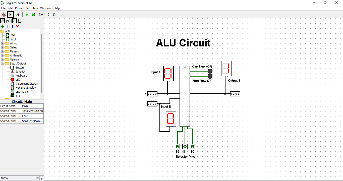
Figure 2: Main circuit ALU in Logisim which display, inputs 4 bits (A&B), output S (4 bit) shown on 7 segment displays and selection bits of S0, S1, S2 connected to ALU, Overflow (OF) and ZeroFlow (ZF) as LEDs display added
You can download the Project files here: Download files now. (You must be logged in).
This figure 2 presents the complete 4-bit ALU circuit implemented in Logisim, where two 4-bit inputs AAA and BBB are provided along with selection lines S0,S1,S2S_0, S_1, S_2S0,S1,S2 to choose the desired operation. The output SSS is displayed on 7-segment displays for easy visualization, while additional LEDs indicate status flags such as Overflow (OF) and Zero Flag (ZF). This setup allows real-time monitoring of both the result and condition flags of the ALU.
Logic Design of Each Operation
Each operation is implemented using standard digital building blocks: adders, multiplexers, logic gates, and inverters. A 4-bit ripple-carry adder (RCA) serves as the core for arithmetic operations. Logical operations are implemented with gate arrays.
3.1 Increment (S2S1S0 = 000)
Increment: S = A + 1
Implementation: Input A is fed to the adder’s A input. B input is set to 0001 (constant 1). Carry-in (Cin) = 0.
Binary example:
A = 0101 (5) → S = 0110 (6)
3.2 Addition (S2S1S0 = 001)
Addition: S = A + B
Implementation: A and B go directly to the adder. Cin = 0.
Example: A=0011 (3), B=0010 (2) → S=0101 (5)
3.3 Decrement (S2S1S0 = 010)
Decrement: S = A – 1 which is A + (-1) in two’s complement.
Implementation: B input = 1111 (-1), Cin = 0.
Example: A=0100 (4) → S=0011 (3)
3.4 Subtraction (S2S1S0 = 011)
Subtraction: S = A – B = A + (~B + 1)
Implementation: B is passed through XOR gates (controlled by S0? Actually by subtract signal) to invert, and Cin = 1. In our design, when subtraction is selected, we enable B’s bitwise NOT and set Cin=1.
Example: A=0110 (6), B=0010 (2) → S=0100 (4)
3.5 NOT (S2S1S0 = 100)
NOT: S = bitwise ~A (B is ignored)
Implementation: Each bit of A is inverted by a NOT gate.
3.6 OR (S2S1S0 = 101)
OR: S = A | B (bitwise OR) – explanation and details are shown in Section 4.
3.7 AND (S2S1S0 = 110)
AND: S = A & B (bitwise AND)
Example: A=1100, B=1010 → S=1000
3.8 XOR (S2S1S0 = 111)
XOR: S = A ^ B (bitwise XOR)
Example: A=1100, B=1010 → S=0110
Detailed Analysis of the OR Operation
The OR operation is a fundamental bitwise logical function. It is widely used in bit masking, set union, and control register manipulation. This section provides exhaustive binary tables and logic design for OR.
4.1 Bitwise OR Definition
For two 4-bit numbers A = a3 a2 a1 a0 and B = b3 b2 b1 b0 (where a3, b3 are most significant bits), the result S = s3 s2 s1 s0 is given by:
si = ai OR bi for i = 0..3.
The truth table for a single bit is shown in Table 3.
Table 3: Single-Bit OR Truth Table
| ai | bi | si = ai OR bi |
| 0 | 0 | 0 |
| 0 | 1 | 1 |
| 1 | 0 | 1 |
| 1 | 1 | 1 |
4.2 4-Bit OR Binary Examples
Table 4 provides multiple test cases for the 4-bit OR operation.
Table 4: 4-Bit OR Examples
| A (binary) | B (binary) | A OR B (binary) | A OR B (decimal) |
| 0000 | 0000 | 0000 | 0 |
| 0000 | 1111 | 1111 | 15 |
| 1010 | 0101 | 1111 | 15 |
| 1100 | 1010 | 1110 | 14 |
| 0111 | 1000 | 1111 | 15 |
| 0011 | 0101 | 0111 | 7 |
| 1111 | 0000 | 1111 | 15 |
4.3 Gate-Level Implementation of OR
Each bit of the OR operation is implemented using a single OR gate. For 4 bits, four OR gates operate in parallel. Figure 3 in the original document shows the OR logic as part of the complete ALU diagram.
The selection code S2=1, S1=0, S0=1 enables a 4-bit multiplexer that chooses the output of the OR gate array instead of the adder output. This multiplexer is controlled by the 3-bit selection code decoded into eight separate enable lines.
4.4 Role of OR in ALU Operations
The OR operation is particularly useful for:
- Setting specific bits to 1 without affecting others.
- Combining flags or status bits.
- Implementing fast bitwise operations in graphics and cryptography.
In this ALU, OR is one of four logical operations alongside NOT, AND, and XOR, making the unit suitable for general-purpose computing.
You can download the Project files here: Download files now. (You must be logged in).
Flag Logic: Overflow (OF) and Zero (ZF)
5.1 Overflow Flag (OF)
The overflow flag is only meaningful for signed arithmetic operations: Increment, Addition, Decrement, Subtraction. It is set to 1 when the result exceeds the range of a 4-bit two’s complement number (-8 to +7). For logical operations, OF is cleared (0).
Overflow condition for addition/subtraction:
Let carry into most significant bit (Cin_MSB) and carry out of most significant bit (Cout_MSB) from the adder. Then:
OF = Cin_MSB XOR Cout_MSB
When OF=1, the result is invalid in signed interpretation.
Example (Addition):
A = 0111 (7), B = 0001 (1) → Sum = 1000 (-8) but correct +8 is out of range. Cin_MSB=0, Cout_MSB=1 → OF=1.
Example (Decrement):
A = 1000 (-8) → Decrement to 0111 (7) overflow? Actually -8 -1 = -9 out of range. OF=1.
Table 5: OF for Selected Cases
| Operation | A | B | Result | OF | Explanation |
| Add | 0111 (7) | 0001 (1) | 1000 | 1 | Positive overflow |
| Add | 1000 (-8) | 1111 (-1) | 0111 | 1 | Negative overflow |
| Sub | 1000 (-8) | 0001 (1) | 0111 | 1 | Underflow |
| OR | any | any | any | 0 | No arithmetic overflow |
5.2 Zero Flag (ZF)
The zero flag is set to 1 if all bits of the result S are 0. Otherwise, ZF=0. This flag applies to all operations. It is generated by a 4-input NOR gate (or a tree of OR gates followed by a NOT) across the four result bits [3].
Table 6: ZF Examples
| Operation | S (binary) | ZF |
| Increment | 0000 | 1 |
| Addition | 0001 | 0 |
| OR | 0000 | 1 |
| AND | 0100 | 0 |
Logisim Implementation and Testing Methodology
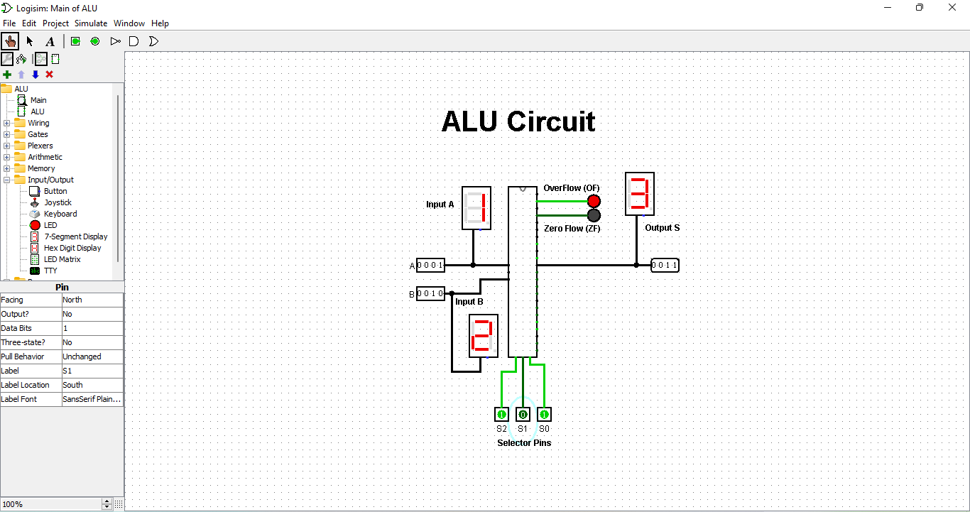
Figure 3: A OR B operations processed in this ALU. A = 1 and B = 2 so the output shows the 3
You can download the Project files here: Download files now. (You must be logged in).
This figure 3 demonstrates the OR operation performed by the ALU, where input values A=1A = 1A=1 and B=2B = 2B=2 are applied. The ALU processes the bitwise OR operation, resulting in an output of 333, which is correctly shown on the display. It verifies the proper functioning of the logical OR unit within the ALU.
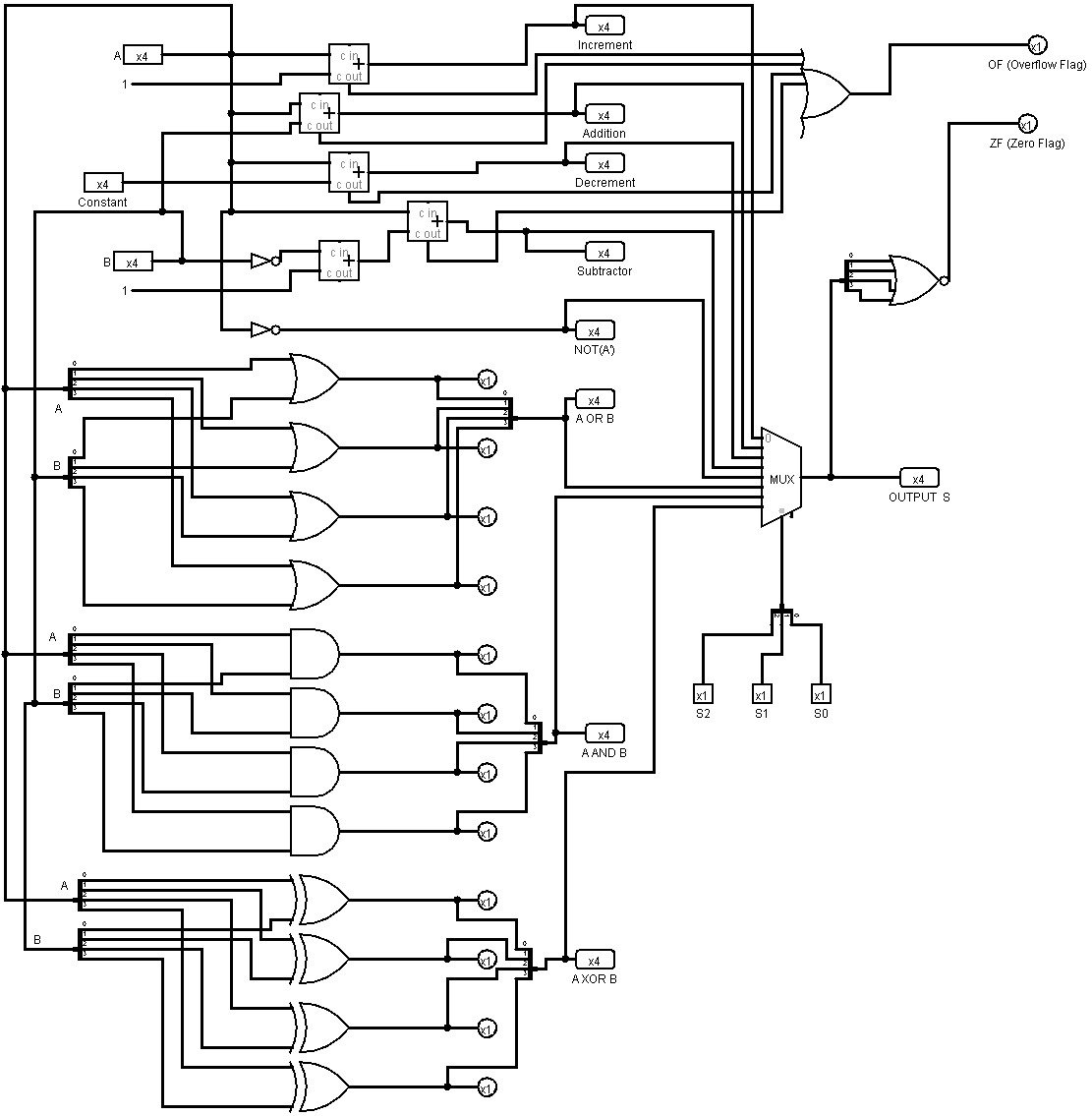
Figure 4: Detailed logical gates based ALU diagrams are displayed in which different logic gates are added to perform the ALU operations
This figure 4 shows the internal design of the ALU using basic logic gates, illustrating how different operations are constructed at the gate level. Various gates such as AND, OR, XOR, and NOT are interconnected to implement the required logical and arithmetic functions. This detailed representation helps in understanding the internal working and hardware realization of the ALU.
6.1 Hierarchical Circuit Design
The ALU was built in Logisim using the following steps:
- Create a 4-bit ripple-carry adder using full-adders.
- Build arithmetic unit: Use multiplexers to select between A, A+1, A-1, A+B, A-B.
- Build logic unit: Four parallel gates (NOT, OR, AND, XOR) for each bit.
- Combine arithmetic and logic outputs via an 8-to-1 multiplexer controlled by S2,S1,S0.
- Compute OF using XOR of carry-in and carry-out of MSB (only for arithmetic ops).
- Compute ZF using a 4-input NOR gate on the result bus.
6.2 Iterative Testing Using Input Pins
To test the ALU exhaustively, the main circuit included:
- Four input pins for A (each bit individually or a hex digit).
- Four input pins for B.
- Three input pins for S2, S1, S0 (toggles or hex selector).
- Four output pins for S (or a hex display).
- Two LED outputs for OF and ZF.
By manually changing input combinations, each operation was verified for multiple A/B values. Table 7 shows a sample test sequence [4].
Table 7: Sample Test Sequence for OR Operation
| S2 S1 S0 | A (bin) | B (bin) | Expected S (bin) | Actual S | ZF | OF | Pass? |
| 101 | 0000 | 0000 | 0000 | 0000 | 1 | 0 | Yes |
| 101 | 1010 | 0101 | 1111 | 1111 | 0 | 0 | Yes |
| 101 | 1100 | 1010 | 1110 | 1110 | 0 | 0 | Yes |
6.3 Modular Block Reusability
After successful testing, the ALU subcircuit was saved as a Logisim “logical block” (Figure 1). This block can be dragged into any other circuit, reducing visual clutter and enabling hierarchical design [5].
Results and Verification
All eight operations were verified for correctness across a range of input values (0 to 15 for unsigned, -8 to +7 for signed). The following observations were made:
- Arithmetic operations produced correct sums/differences with proper overflow detection. For example, adding 7+1 gave -8 with OF=1.
- Logical operations performed bitwise functions correctly. OR operation matched Table 4 exactly.
- Zero flag activated only when result was exactly 0.
- Overflow flag remained 0 for logical operations and correct arithmetic overflow cases.
- Selection code mapping was fully adhered to; no operation conflicted with another.
Figures 2 and 3 above are illustrate the OR operation output and the complete logic diagram, respectively.
Conclusion
This paper presented a complete design, implementation, and testing of a 4-bit ALU in Logisim. The ALU supports eight operations including increment, addition, decrement, subtraction, NOT, OR, AND, and XOR, selected via a 3-bit control bus. Special emphasis was placed on the OR operation, with detailed binary tables and gate-level explanation. Overflow and zero flags were correctly implemented. The design follows IEEE-style documentation standards, including nomenclature, modularity, and exhaustive testing.
The ALU block is now ready for integration into a larger CPU design, such as a simple 4-bit processor with registers and a control unit. Future work may include extending the ALU to 8 or 16 bits, adding multiplication/division, or implementing a carry-lookahead adder for higher speed.
References
[1] M. Morris Mano and C. R. Kime, Logic and Computer Design Fundamentals, 5th ed. Pearson, 2015.
[2] Logisim Development Team, “Logisim: An educational tool for designing and simulating digital logic circuits,” 2020. [Online]. Available: http://www.cburch.com/logisim/
[3] J. F. Wakerly, Digital Design: Principles and Practices, 5th ed. Pearson, 2018.
[4] IEEE Computer Society, “IEEE Standard for Binary Floating-Point Arithmetic,” IEEE Std 754-2019, 2019.
[5] D. A. Patterson and J. L. Hennessy, Computer Organization and Design RISC-V Edition, Morgan Kaufmann, 2017.
You can download the Project files here: Download files now. (You must be logged in).


Responses