

A High Efficiency, Ka-Band, GaN-on-SiC MMIC with Low Compression
Author: Waqas Javaid
Abstract
The design and performance of a 28 V, 3-stage, Ka- band, GaN-on-SiC, power amplifier MMIC with high efficiency and low gain compression are presented. At 30 GHz, the MMIC provides saturated power of 37.6 dBm with an associated PAE of 39.8%. P1dB is within 1 dB of saturated power over the 26.5 30.5 GHz band. At 30 GHz, P1dB is 37.1 dBm with an associated PAE of 37.8%. In addition, the MMIC has a low quiescent bias of 72 mA.
I. Introduction
The demand for more bandwidth is creating more commercial applications for the Ka-band. Satellite communications, point-to-point communications, 5G, and military radar are all applications that use or plan to use the Ka- band. The high power density and high breakdown voltage of GaN-on-SiC make it of particular interest for power amplifiers. Wolfspeed has developed a leading 150 nm, GaN-on-SiC process using an optically defined, i-line gate.[1,2] The purpose of this work is to demonstrate the capabilities of this process by designing a 3-stage, 28 V, Ka-band, power amplifier MMIC. Most GaN power amplifiers start compressing well before saturated power is achieved. This MMIC power amplifier displays high efficiency, low quiescent bias, and low gain compression representing an improvement in the state of the art.
II. ProccessTechnology
The GaN-on-SiC substrate and epitaxy are optimized for 30 GHz RF performance and 28 V operation. The 150 nm gate is optically defined using an i-line lithography spacer method. High Temperature Reverse Bias (HTRB) stress tests were performed to confirm the robustness and reliability of the process technology. The HEMT devices were subjected to 84 V HTRB for 1000 hours with negligible performance degradation and zero device fails. The substrate thickness is 75 µm. Through substrate vias are available and can be placed within 50 µm of each other. The MMIC process also includes 180 pF/mm2 MIM capacitors, 12 Ω/sq thin film resistors, and vias in the HEMT source pads. [1] The IDSS0 for the process is approximately 700 mA/mm.
III. Circuit Design
The target frequency range for the MMIC PA was 26.5- 30.5 GHz. This frequency range was selected to cover several potential 5G millimeter wave bands. Other design goals included a saturated power greater than 4 W, at least 25 dB of small-signal gain, and PAE greater than 30% over the band. In addition, low gain compression was desired for better P1dB than a typical 3-stage GaN amplifier.
The MMIC PA has 3 stages. The first stage is a 6×50 µm device, the second stage has two 6×50 µm devices, and the third stage has four 6×50 µm devices. This constitutes a 1:2 drive ratio for each stage. Typical GaN amplifiers have considerable gain compression and can start compressing well before saturated power (Psat) is achieved. Part of the design goal for this MMIC was to improve the 1 dB compression power (P1dB) compared to typical 3- stage, high-efficiency, GaN amplifiers. To accomplish this, the first stage is biased separately from the last two stages and is biased in class A mode, which also helps to increase gain. The last two stages are biased in class AB mode for efficiency. The first stage is biased at 36 mA, which corresponds to 120 mA/mm. The last two stages are biased at 20 mA/mm, for a combined 36 mA. The overall quiescent current of the
You can download the Project files here: Download files now. (You must be logged in).
amplifier is 72 mA. The class A first stage tends to provide gain compression, while the class AB operation of the last two stages tend to provide gain expansion. These two different effects are used to reduce the soft gain compression that is typically found in a GaN amplifier. The drain voltage for the design and operation is 28 V.
The output load impedance is determined by load pull data and circuit simulation. The matching networks have high pass and low pass elements to provide a broad band of operation.
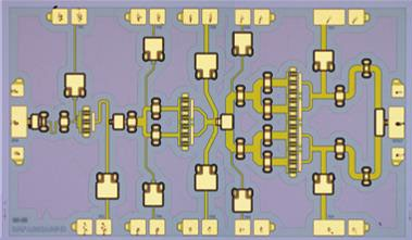
EM simulation and tuning are used to optimize the matching circuits for the best overall circuit performance. A photo of the completed MMIC is shown in Fig. 1.
You can download the Project files here: Download files now. (You must be logged in).
IV. Measured Results
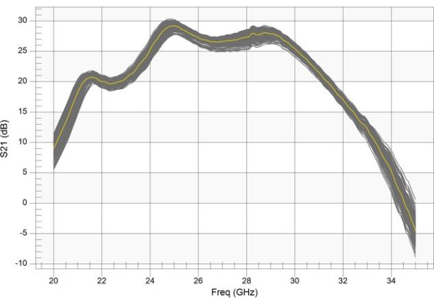
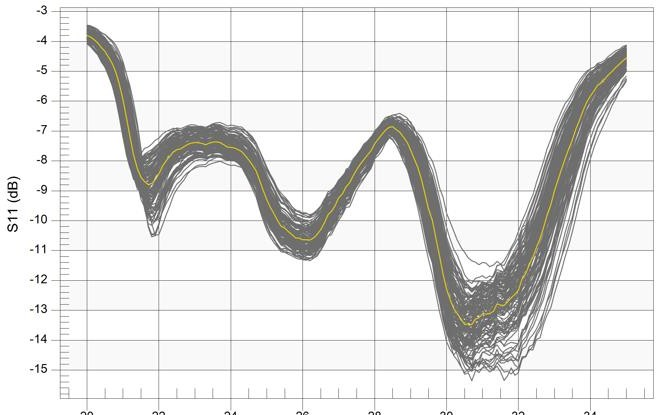
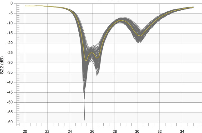
After wafer fabrication, the S-parameters are measured on- wafer. The S-parameters shown here are measured on 120 devices across a wafer. The yellow line represents the mean of

the data, and the gray lines represent the individual devices. Figure 2 shows S21, Fig. 3 shows S11, and Fig.4 shows S22. The S-parameters indicate very good broad band performance.
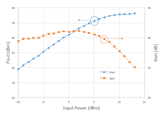
Power sweep testing was done on 5 devices across the wafer from 26 GHz to 30.5 GHz. The power and PAE results presented are the averages of these 5 devices. Power measurements were done on-wafer using a power pulse. The duty- cycle of the pulse is 1% and the duration was 10 µs. These are standard on-wafer pulsed-power parameters for Wolfspeed to avoid over heating the wafers during testing. Figure 5 shows output power (Pout) versus input power (Pin) at 28.5 GHz, the middle of the band. The associated gain versus input power is also plotted in Fig. 5. The gain is relatively flat over swept input power, which is desirable for linearity.
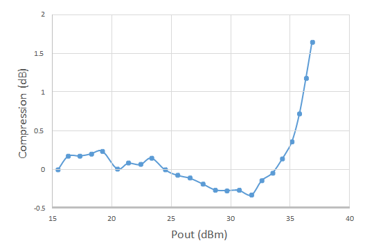
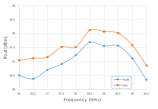
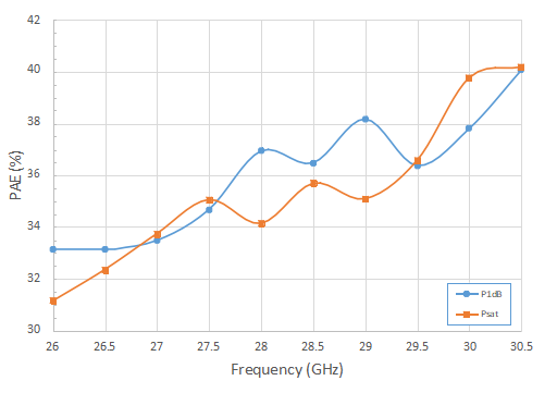
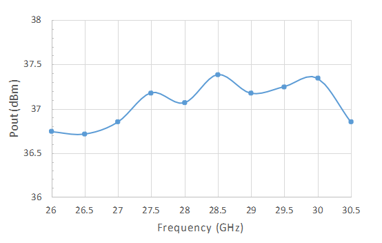
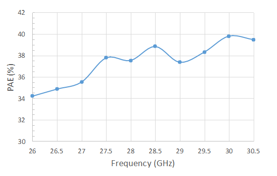
Figure 6 shows output power (Pout) at maximum PAE over the band, and the corresponding maximum PAE is shown in Fig. 7. The 4 W output power and 30% PAE goals have been exceeded.PAE is excellent across the band and approaches 40% at 30 GHz. The PAE measurements compare very favorably with previously published results. A comparison of power and PAE to previously published work is shown in Table 1. [3-7]
You can download the Project files here: Download files now. (You must be logged in).
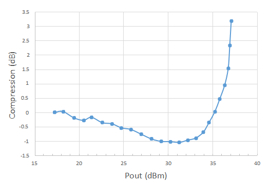
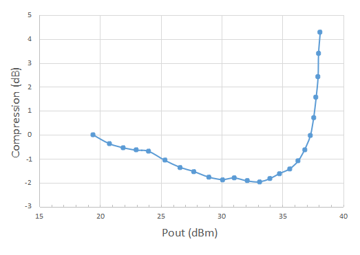
Gain compression measurements averaged over 5 devices are shown at 26.5 GHz, 28.5 GHz, and 30.5 GHz in Fig. 8, Fig. 9, and Fig. 10 respectively. All of the figures show some gain expansion followed by gain compression. Typical GaN amplifiers have soft gain compression that starts well before Psat. These plots show a quick transition from P1dB to Psat. Gain expansion can impact linearity, just as gain compression can impact linearity. The amount of impact depends on the type of modulation. A parameter such as third-order intermodulation distortion (IM3) will be sensitive to the slope of the gain with respect to input power. The gain expansion observed is modest and has a gentle slope. As a result, the sharp slope of the gain compression still dominates.
Figure 11 compares P1dB and Psat across frequency. P1dB is within 1 dB of Psat across the band, which is an excellent result for a GaN MMIC PA. The PAE for Psat and for P1dB are shown in Fig. 12. PAE at P1dB is very good across the band. PAE at P1dB is 37.8% at 30 GHz. To the authors’ knowledge, this is the highest reported PAE at P1dB for a 3-stage GaN power amplifier MMIC operating in the Ka-band.
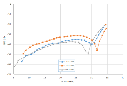
The IM3 for a device was measured under CW conditions and the results are shown in Fig. 13. We like to see IM3 less than -25 dBc for a GaN amplifier. This is achieved at powers levels within 4 dB of Psat, which is considered to be a good result.
V. Conclusions
The results for a 28 V, 3-stage, Ka-Band, GaN-on-SiC, MMIC power amplifier using an optically defined, i-line 150 nm gate are reported. The MMIC provides a saturated power of 37.6 dBm with an associated PAE of 39.8% at 30 GHz. The MMIC exhibits low gain compression, excellent P1dB, and low quiescent bias. P1dB is within 1 dB of Psat over the 26.5 -30.5 GHz band. At 30 GHz, P1dB is 37.1 dBm with an associated PAE of 37.8% and quiescent bias of 72 mA. To the authors’ knowledge, this is the highest reported efficiency at P1dB for a Ka-band, 3-stage MMIC.
References
- Bothe et al., “Optically-Defined 150-nm, 28-V GaN HEMT Processfor Ka- and,” 2019 CS MANTECH TECHNICAL DIGEST, May 2019.
- Wood et al., “An Optical 0.25 um GaN HEMT Technology on 100 mm SiC for RF Discrete and Foundry MMIC Products,” 2013 CS MANTECH TECHNICAL DIGEST, May 2013.
- Campbell et al., “High Efficiency Ka-Band Gallium Nitride PowerAmplifier MMICs,” 2013 IEEE Internatial Conference on Microwaves, Communications, Antennas and Electronic Systems (COMCAS), Oct. 2013.
- Din et al., “High Power and High Efficiency Ka Band PowerAmplifier,” 2015 IEEE Internal Microwave Symposium (IMS), May 2015.
- Cheron et al., “High-gain Over 30% PAE Power Amplifier MMICs in100 nm GaN Technology at Ka-Band Frequencies,” Proceedings of the 10th European Microwave Integrated Circuits Conference, Sept. 2015.
- Blount et al., “A High Efficiency, Ka-Band Pulsed Gallium NitridePower Amplifier for Radar Applications,” 2016 IEEE Compound Semiconductor Integrated Circuit Symposium (CSICS), Oct. 2016.
- Roberg et al., “40W Ka-Band Single and Dual Output GaN MMICPower Amplifiers on SiC,” 2018 IEEE BiCMOS and Compound Semiconductor Integrated Circuits and Technology Symposium (BCICTS), Oct. 2018.
You can download the Project files here: Download files now. (You must be logged in).


Responses