

Boost Converter with PFC and Thermal Model development in PLECS
Author: Waqas Javaid
Abstract
This paper presents the modeling, control, and thermal analysis of a 300 W grid-connected boost converter with Power Factor Correction (PFC) developed in PLECS Standalone. The proposed switched-mode power supply operates from a wide AC input voltage range of 85 Vrms to 265 Vrms and regulates the output voltage at 390 V DC. The system integrates the electrical power stage, cascaded current and voltage control loops, and semiconductor thermal behavior within a unified simulation environment. The power circuit consists of a diode bridge rectifier followed by a continuous conduction mode (CCM) boost converter using an Infineon Technologies CoolMOS MOSFET and a Silicon Carbide (SiC) Schottky diode to improve conversion efficiency and reduce switching losses. The control architecture is based on the ICE1PCS01 PFC controller implementing average current-mode control through an inner current loop and an outer voltage regulation loop. Thermal modeling of the MOSFET and boost diode is achieved using datasheet-based thermal impedance networks and RC thermal equivalent circuits. Simulation results demonstrate stable startup behavior, sinusoidal input current shaping, controlled output voltage regulation, and realistic semiconductor junction temperature evolution under load conditions. Furthermore, steady-state thermal analysis significantly reduces computational time compared to long transient simulations. The presented model provides a practical framework for evaluating electrical, control, efficiency, and thermal characteristics of high-performance PFC boost converters for industrial power supply applications.
Introduction
Power factor correction (PFC) converters have become an essential part of modern switched-mode power supplies due to increasingly strict electromagnetic compatibility (EMC) regulations and energy efficiency requirements in industrial, commercial, and consumer electronic systems. Conventional diode rectifier-capacitor front-end circuits draw highly distorted input currents from the AC mains, resulting in poor power factor, increased harmonic distortion, and reduced system efficiency. To overcome these limitations, boost converter based active PFC topologies are widely adopted because they provide nearly sinusoidal input current waveforms while maintaining regulated high-voltage DC outputs over wide input voltage ranges. Among the various control strategies, average current-mode control operating in continuous conduction mode (CCM) offers excellent current shaping performance, low harmonic distortion, and improved dynamic response under varying load conditions.
This project presents a detailed simulation and thermal analysis of a 300 W boost converter with active power factor correction implemented in PLECS Standalone. The converter operates from universal AC input voltages ranging from 85 Vrms to 265 Vrms and delivers a regulated 390 V DC output suitable for industrial switched-mode power supply applications. The system integrates the electrical power stage, cascaded control loops, and semiconductor thermal behavior within a single simulation framework, allowing simultaneous investigation of electrical and thermal performance. The boost converter utilizes high-efficiency semiconductor devices including an Infineon Technologies CoolMOS MOSFET and a Silicon Carbide (SiC) Schottky diode to minimize switching and conduction losses at elevated switching frequencies.
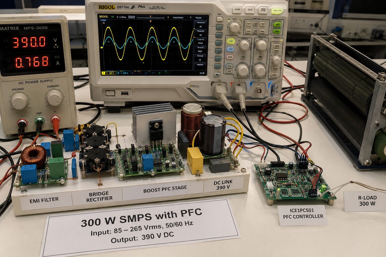
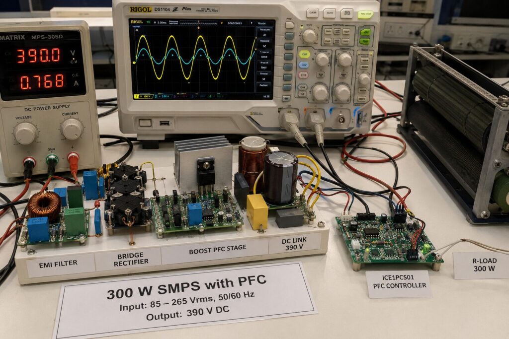
Figure A: 300 W boost converter with active power factor correction implemented in PLECS Standalone and real PCB design
Figure A presents the 300 W boost converter and PFC which implemented by PLECS software and its real time PCB testing in research lab of bahria university islamabad. The controller architecture is based on the ICE1PCS01 PFC control IC, which employs cascaded control consisting of an inner current loop and an outer voltage loop. The inner loop ensures that the average input current follows the shape of the input voltage waveform, thereby improving the input power factor and reducing harmonic distortion. The outer voltage loop regulates the DC bus voltage while suppressing the low-frequency ripple produced by rectified AC mains operation. In addition to electrical modeling, this work also incorporates detailed thermal descriptions of the semiconductor devices using thermal RC equivalent networks and manufacturer datasheet information. Thermal analysis is particularly important in high-power converters because semiconductor losses directly influence device reliability, efficiency, and heat sink design requirements. The integrated electro-thermal simulation environment enables accurate prediction of junction temperatures, switching losses, conduction losses, and overall converter efficiency under dynamic operating conditions.
The presented study demonstrates the startup response, steady-state operation, thermal transients, and steady-state thermal analysis of the converter under constant load conditions. The results validate the effectiveness of combining power electronics, control systems, and thermal modeling into a unified simulation platform for advanced switched-mode power supply design and optimization.
2. Design Methodology
The design methodology of the proposed boost converter with power factor correction follows an integrated electro-thermal modeling approach implemented in PLECS Standalone. The overall system consists of three major sections: the electrical power circuit, the cascaded control system, and the thermal modeling subsystem. The electrical stage begins with a single-phase AC input followed by an electromagnetic interference (EMI) filter implemented in a CLC configuration to suppress high-frequency switching noise and conducted emissions generated by the boost converter. The filtered AC voltage is rectified using a full-bridge diode rectifier to produce an unregulated DC voltage, which serves as the input to the active boost PFC stage. The boost converter is designed to maintain a regulated output voltage of 390 V DC while operating across a wide input voltage range from 85 Vrms to 265 Vrms. To achieve high conversion efficiency and reduced switching losses, the converter employs an Infineon Technologies CoolMOS power MOSFET and a Silicon Carbide (SiC) Schottky boost diode [1].
The control system is implemented using an average current-mode control architecture based on the ICE1PCS01 PFC controller model. The control structure consists of two cascaded feedback loops: an inner current loop and an outer voltage loop. The inner current loop regulates the average inductor current and forces it to follow the instantaneous input voltage waveform, thereby achieving near-unity power factor and low total harmonic distortion (THD). The duty cycle of the pulse-width modulation (PWM) signal is continuously adjusted according to the input voltage and current feedback signals. Under heavy load conditions, the converter operates in continuous conduction mode (CCM), whereas under lighter loads the system may transition into discontinuous conduction mode (DCM) depending on the boost inductor current profile. The outer voltage loop regulates the DC bus voltage at 390 V and suppresses the double-line-frequency ripple component present at the converter output. Compensation networks connected to the controller ensure loop stability and prevent amplification of low-frequency ripple components within the feedback system.
Thermal modeling forms a critical part of the design methodology because semiconductor temperature strongly affects converter efficiency, switching behavior, and long-term reliability. The thermal behavior of the MOSFET and SiC diode is modeled using manufacturer datasheet-based thermal impedance characteristics and RC thermal equivalent circuits. The thermal model includes junction-to-case, case-to-heat-sink, and heat-sink-to-ambient thermal paths. Switching and conduction losses generated by the semiconductor devices are transferred into the thermal network, where thermal capacitances simulate heat accumulation and thermal resistances model heat dissipation to the ambient environment. The heat sink assembly is shared between multiple semiconductor devices to emulate realistic thermal coupling effects found in practical converter hardware implementations. In addition, steady-state thermal analysis tools available in PLECS are used to rapidly determine the long-term thermal operating point without requiring excessively long transient simulations. This integrated electro-thermal methodology enables accurate evaluation of converter efficiency, thermal stability, device stress, and dynamic performance under different operating conditions.
You can download the Project files here: Download files now. (You must be logged in).
3. PLECS Simulation with its Results
This demonstration shows a 300 W switched-mode power supply. The AC input voltage may vary be-tween 85 Vrms and 265 Vrms. The controlled output voltage is 390 V DC.
The simulation combines the electrical power circuit, the control with a standard IC and the thermal behavior of the semiconductors.
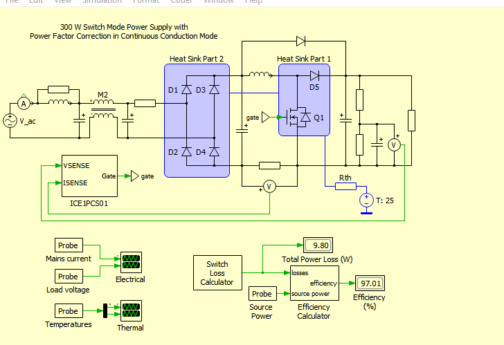
Figure 1: 300 W Switch Mode Power Supply with Power Factor Correction (PLECS Standalone)
This figure 1 illustrates the complete 300 W switched-mode power supply (SMPS) model developed in PLECS Standalone with integrated Power Factor Correction (PFC) and thermal analysis capabilities. The system accepts a wide-range single-phase AC input voltage from 85 Vrms to 265 Vrms and converts it into a regulated 390 V DC output suitable for industrial and power electronic applications. The model combines the electrical power stage, cascaded control loops, PWM switching logic, and thermal behavior of semiconductor devices within a unified simulation environment.
The input stage consists of an EMI filter in CLC configuration followed by a diode bridge rectifier that converts the AC mains voltage into an unregulated DC waveform. The rectified voltage feeds the boost PFC converter, which uses an Infineon CoolMOS MOSFET and a Silicon Carbide (SiC) Schottky diode to improve efficiency and reduce switching losses. The converter operates in Continuous Conduction Mode (CCM) under normal loading conditions and is controlled using the ICE1PCS01 PFC controller model implemented with functional blocks.
The figure 1 also demonstrates the cascaded control structure composed of an inner current loop and an outer voltage loop. The inner loop shapes the input current to follow the sinusoidal input voltage waveform, thereby improving the power factor and minimizing harmonic distortion. The outer loop regulates the DC output voltage at 390 V despite variations in input voltage and load conditions. Integrated thermal models are included for the MOSFET, boost diode, and heat sink, enabling simultaneous electrical and thermal performance analysis during converter startup and steady-state operation.
3.1. Model description
The proposed switched-mode power supply is designed using a boost converter topology integrated with an active Power Factor Correction (PFC) stage. The complete system is modeled and simulated in PLECS Standalone to analyze both electrical and thermal behavior under different operating conditions. The converter is intended for medium-power industrial applications where high efficiency, low harmonic distortion, and reliable thermal performance are essential. The overall model consists of two major sections: the power circuit and the control system.
3.1.1. Power circuit
The power supply is based on a diode rectifier and a power factor correction circuit in boost topology. After having passed the input EMI filter in CLC configuration, the single-phase line voltage is rectified by a standard diode bridge. To improve the efficiency, the boost converter is realized with an Infineon CoolMOS power switch and a Silicon Carbide (SiC) Schottky diode.
3.1.2. Control System
In PLECS Standalone the controller IC [1] and plant are modeled with functional blocks in individual subsystems. It operates in continuous conduction mode (CCM) with av-erage current control. For PLECS Blockset the controller is implemented on the Simulink level.
The control is cascaded and consists of the inner current loop and the outer voltage loop.
- The inner current loop controls the sinusoidal profile for the average input It uses the dependency of the PWM duty cycle on the line input voltage to determine the corresponding input cur-rent. This means the average input current follows the input voltage as long as the device operates in CCM. Under light load condition, depending on the choke inductance, the system may enter into discontinuous conduction mode (DCM). In DCM, the average current waveform will be slightly distorted.
- The outer voltage loop controls the output bus The output voltage contains a ripple with double the frequency of the input voltage (e.g. 120 Hz in North America). A compensation network connected to the IC suppresses this ripple which must not be amplified by the control loop.
The mask of the controller block contains the parameters of passive components that in reality are directly connected to the IC. The switching frequency can be specified directly, although in reality it is programmed via an external resistor.
The model of the control IC supports soft start for low output voltage. However, other protection features such as over-voltage and peak current protection are not implemented.
3.1.3. Thermal model
Datasheet information for Infineon’s SPP20N60C3 CoolMOS MOSFET and SDP04S60 SiC Schottky diode has been used to populate the loss look-up tables in the thermal descriptions.
A special component model is used to simulate the thermal behavior of the MOSFET. Look under the mask of this component to see the thermal equivalent circuit of the device:
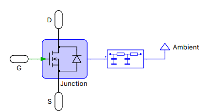
Figure 2: MOSFET Model with body diode and thermal description
You can download the Project files here: Download files now. (You must be logged in).
This figure 2 presents the detailed electro-thermal model of the power MOSFET used in the boost Power Factor Correction (PFC) converter developed in PLECS Standalone. The model includes both the electrical switching characteristics of the MOSFET and the thermal behavior of the semiconductor device during converter operation. In addition to the main MOSFET switch, the model also incorporates the intrinsic body diode, which becomes active during reverse current conditions and contributes to conduction and switching losses.
The thermal section of the model is represented using an equivalent thermal RC network that simulates heat flow from the semiconductor junction to the device case and finally to the external heat sink and ambient environment. The thermal capacitance models the heat storage capability of the semiconductor chip, while the thermal resistances represent heat transfer paths through the package and cooling structure. This arrangement allows accurate prediction of junction temperature rise under varying electrical loading and switching conditions.
The figure 2 also demonstrates how switching losses and conduction losses generated within the MOSFET are converted into thermal energy and propagated through the thermal network. The temperature feedback from the thermal model influences the electrical behavior of the device, enabling realistic electro-thermal interaction analysis. Such integrated thermal modeling is essential for evaluating device reliability, heat sink sizing, efficiency optimization, and safe operating limits in high-power switched-mode power supplies.
Within the MOSFET model, the heat sink (i.e. the blue frame) represents the thermal capacitance of the chip. It collects all switching loss energy and conduction loss power from the dies of the MOSFET and the reverse diode. It also propagates its temperature back to the chip in order to receive the cor-rect loss readings. The losses are propagated via a thermal RC chain which models the case of the component. The Ambient Temperature component at the end connects the component with an outside heat sink modeling the dissipator that the component is mounted on.
These descriptions can be viewed and edited by double-clicking on the component and selecting Edit… from the drop-down menu of the Thermal description parameter. In the SiC boost diode model, the thermal impedance of the device has been entered directly in the thermal description:
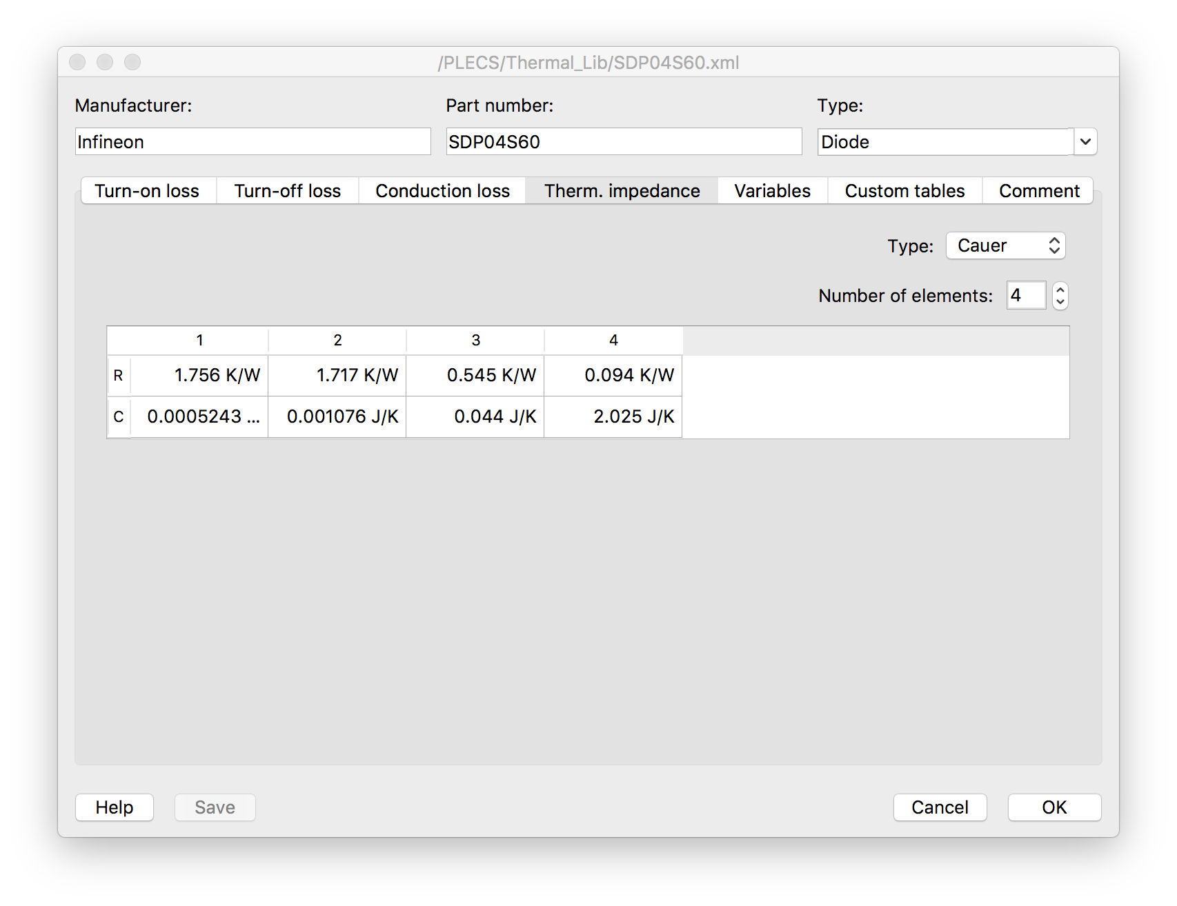
Figure 3: Thermal impedance of SiC boost diode model
This figure 3 illustrates the thermal impedance network used to model the heat dissipation characteristics of the Silicon Carbide (SiC) boost diode in the PFC converter. The thermal model represents the heat flow from the diode junction to the ambient environment through equivalent thermal resistances and capacitances, enabling accurate prediction of junction temperature during switching and conduction operation. Such modeling is important for analyzing thermal stability, efficiency, and long-term reliability of high-frequency power electronic converters.
In the main circuit it can be seen that the dissipator is split into two heat sink frames in order to com-prise both the rectifier diodes and the semiconductors of the PFC stage. A thermal resistance connects the dissipator with the temperature of the ambient air.
- The thermal descriptions for the MOSFET and diodes are stored in a private thermal library in the PLECS.
- The average switching, conduction and total losses of the semiconductor devices can be calculated easily using the “Switch Loss Calculator” Select the switch components of interest in the schematic editor and drag them onto the probed components list of the “‘Switch Loss Calculator” block. For more details, browse the Help section of this block.
- The “Efficiency Calculator” subsystem calculates the converter efficiency using the source power and total switch losses.
- For more information on thermal modeling and the calculation of device losses and efficiency, see the demo model “Buck Converter with Thermal Model” in the PLECS demo models library.
4. Simulation and Testing
The simulation shows a start-up of the power supply under constant load. Fig. 4 with the electrical quantities shows the sinusoidal mains current and the ramp-up of the output voltage. A 120 Hz ripple in the output voltage can be observed. Fig. 5 shows the junction temperature of the MOSFET (green) and the boost diode (red). The temperature of the external heat sink is rising very slowly in the time frame of the simulation.
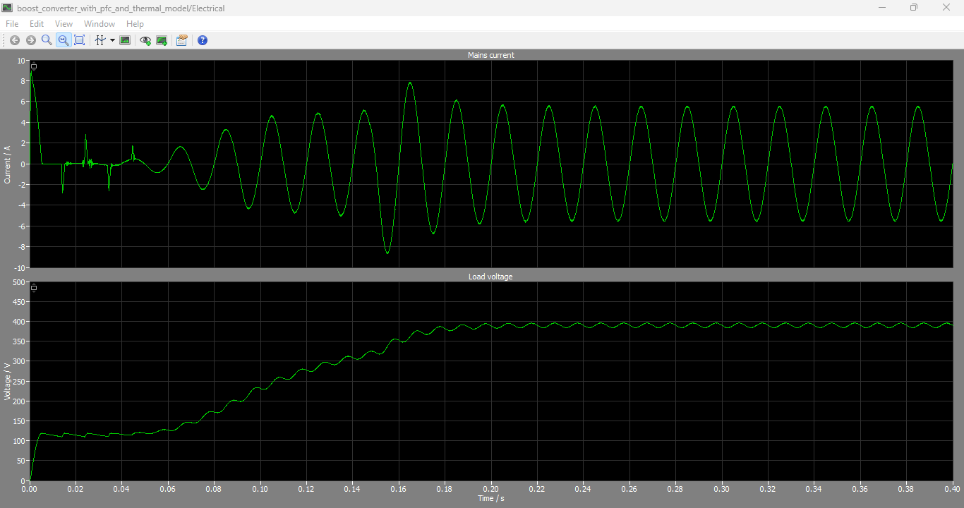
Figure 4: Electrical behavior during start-up of the power supply under constant load
You can download the Project files here: Download files now. (You must be logged in).
This figure 4 shows the transient electrical response of the PFC boost converter during startup under a fixed load condition. The output voltage gradually rises as the control loop regulates the DC bus toward its nominal value of 390 V, while the input current follows a sinusoidal waveform shaped by the PFC control. During this period, the system transitions from initial charging of passive components to steady-state operation. The observed behavior confirms proper functioning of both the inner current control loop and outer voltage regulation loop.
4.1. Steady-state operation
It is not practical to determine the stationary temperature levels of the dissipator and the semiconductors by running a simulation until the thermal transients have settled. Due to the large thermal time constants such a simulation would take several hours.
Instead, you can perform a Steady-State Analysis that is pre-configured in the model. For PLECS Standalone or Blockset (in Simulink) execute the following steps:
- Standalone: From the Simulation menu choose Analysis This opens a dialog, in which the
analysis has already been pre-configured. To start the analysis, click on the Start analysis button. You can display the progress of the analysis by clicking on the Show log button.
- Blockset: Double-click on the Steady-State Analysis block to open the dialog and click on the Start analysis The progress of the analysis is displayed in the MATLAB Command Window.

Figure 5: Thermal behavior during start-up of the power supply under constant load
This figure 5 shows the transient thermal response of the power semiconductor devices during the start-up phase of the 300 W PFC boost converter modeled in PLECS Standalone. As the converter energizes under constant load, the junction temperatures of the MOSFET and SiC diode gradually rise due to switching and conduction losses. The heat sink temperature increases more slowly because of its larger thermal time constant. This behavior highlights the dynamic interaction between electrical power dissipation and thermal accumulation in the system.
When the analysis has finished a simulation of five steady-state cycles is displayed for all waveforms preconfigured in the Scopes.
5. Conclusion
This PLECS model shows a grid-connected boost converter with PFC and thermal modeling. The system is controlled by an IC from Infineon, which is modeled with functional blocks in a separate sub-system. The control is cascaded and consists of the inner current loop and the outer voltage loop. To describe the thermal behavior of the MOSFET and the boost diode, thermal descriptions were added in the component parameters. Due to the large thermal time constants a transient simulation would take several hours to reach steady-state. Instead, you can perform the Steady-State Analysis on the circuit, which finds the steady-state within seconds.
References
[1] In PLECS Standalone, the Power Factor Correction (PFC) controller was modeled based on the ICE1PCS01 Continuous Conduction Mode (CCM) PFC Controller IC from Infineon Technologies.
You can download the Project files here: Download files now. (You must be logged in).


Responses