

Power Amplifier Design in LTSpice and Altium for Piezo Ultrasonic Transducers
Abstract
This report presents the design and implementation of a high-voltage, high-efficiency power amplifier for driving piezoelectric ultrasonic transducers operating in resonance. The amplifier is designed to deliver a stable 300V peak-to-peak (106 Vrms) output at a maximum current of 6A, across a purely resistive 25-ohm load. The design accommodates both square and sine wave inputs over a frequency range of 1kHz to 2MHz with a 10% duty cycle, making it suitable for high-frequency ultrasonic applications. LTSpice was employed for circuit simulation and validation, while Altium Designer was used to develop the PCB layout. The system was tested under laboratory conditions with real piezo transducers to evaluate its stability, thermal performance, and output integrity.
1. Introduction
Power amplifiers for piezoelectric ultrasonic transducers require high voltage and current outputs, broad bandwidth operation, and stable response under capacitive or resonant loading. These devices are critical in medical imaging, industrial cleaning, and ultrasonic sensing systems. The challenge lies in designing an amplifier that not only amplifies low-voltage signals to hundreds of volts but also operates efficiently across a wide frequency range without distortion or instability [1].
This project aims to design, simulate, and prototype a power amplifier capable of delivering 300Vpp across a 25-ohm load with up to 6A of peak current, accepting inputs in the form of square or sine waves from a signal generator. LTSpice was utilized for schematic simulation and optimization, and Altium Designer was used for PCB development and layout. The amplifier is ultimately integrated with ultrasonic piezo transducers to test its real-world application performance [2].
2. Methodology
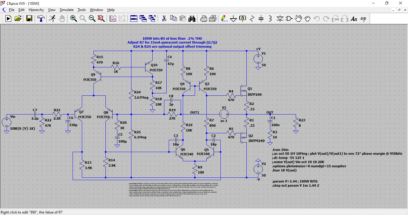
2.1 Circuit Design in LTSpice
The amplifier circuit was initially modeled in LTSpice to verify its capability to meet the required electrical specifications:
– Input: 1Vrms square/sine wave
– Output: 300V peak-to-peak at 25Ω load
– Bandwidth: 1kHz – 2MHz
– Current Handling: Up to 6A
– Duty Cycle: 10%
Key Design Aspects:
– Topology: A Class D or high-voltage push-pull amplifier was explored due to its switching efficiency and ability to handle reactive loads [3].
– Simulation: Frequency response, transient analysis, and harmonic distortion were evaluated.
– Feedback: Negative feedback was introduced to improve gain stability and reduce THD (Total Harmonic Distortion).
2.2 Component Selection
Component selection was based on simulation results and real-world constraints:
– MOSFETs: High-speed, high-voltage MOSFETs capable of handling >400V drain-source voltage and pulsed currents up to 10A were selected (e.g., IRFP460).
– Driver ICs: Gate driver ICs like the IR2110 were chosen to provide fast switching and isolation.
– Capacitors/Inductors: RF-rated capacitors and low-ESR inductors were selected for signal integrity at high frequencies.
– Resistors: Power resistors and precision sense resistors were used in the feedback network.
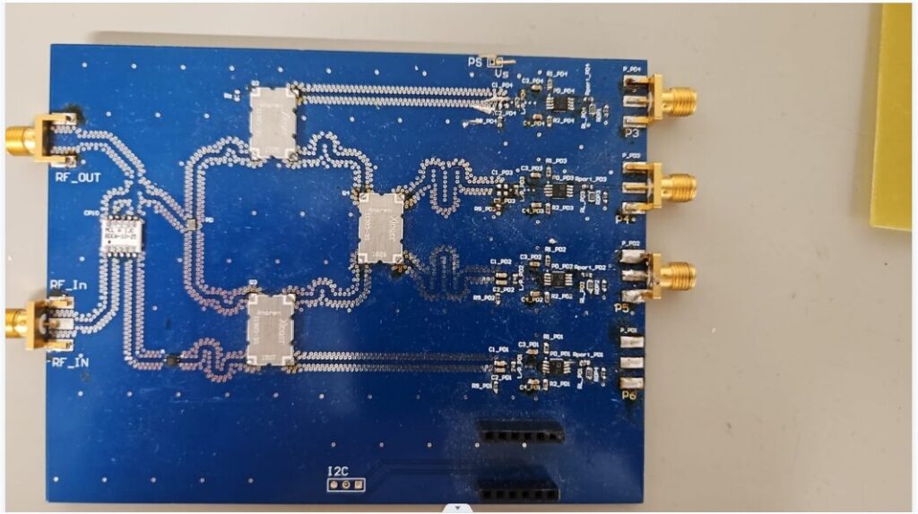
2.3 PCB Design in Altium Designer
A compact and thermally managed PCB was developed using Altium:
– Layering: 2-layer PCB with proper separation of high-voltage and low-voltage sections.
– Grounding: Star grounding and low-impedance return paths were ensured to minimize EMI and noise coupling.
– Thermal Management: Heat sinks and copper pours were added for MOSFET thermal dissipation [4].
– Trace Widths: Calculated based on IPC-2221 standards to carry 6A peak without overheating.
3. Testing and Validation
3.1 Test Parameters:
– Input Signals: 1Vrms square and sine waves
– Load: 25-ohm resistive load and equivalent piezo transducer
– Measurement Equipment: Oscilloscope, current probe, thermal camera, frequency analyzer
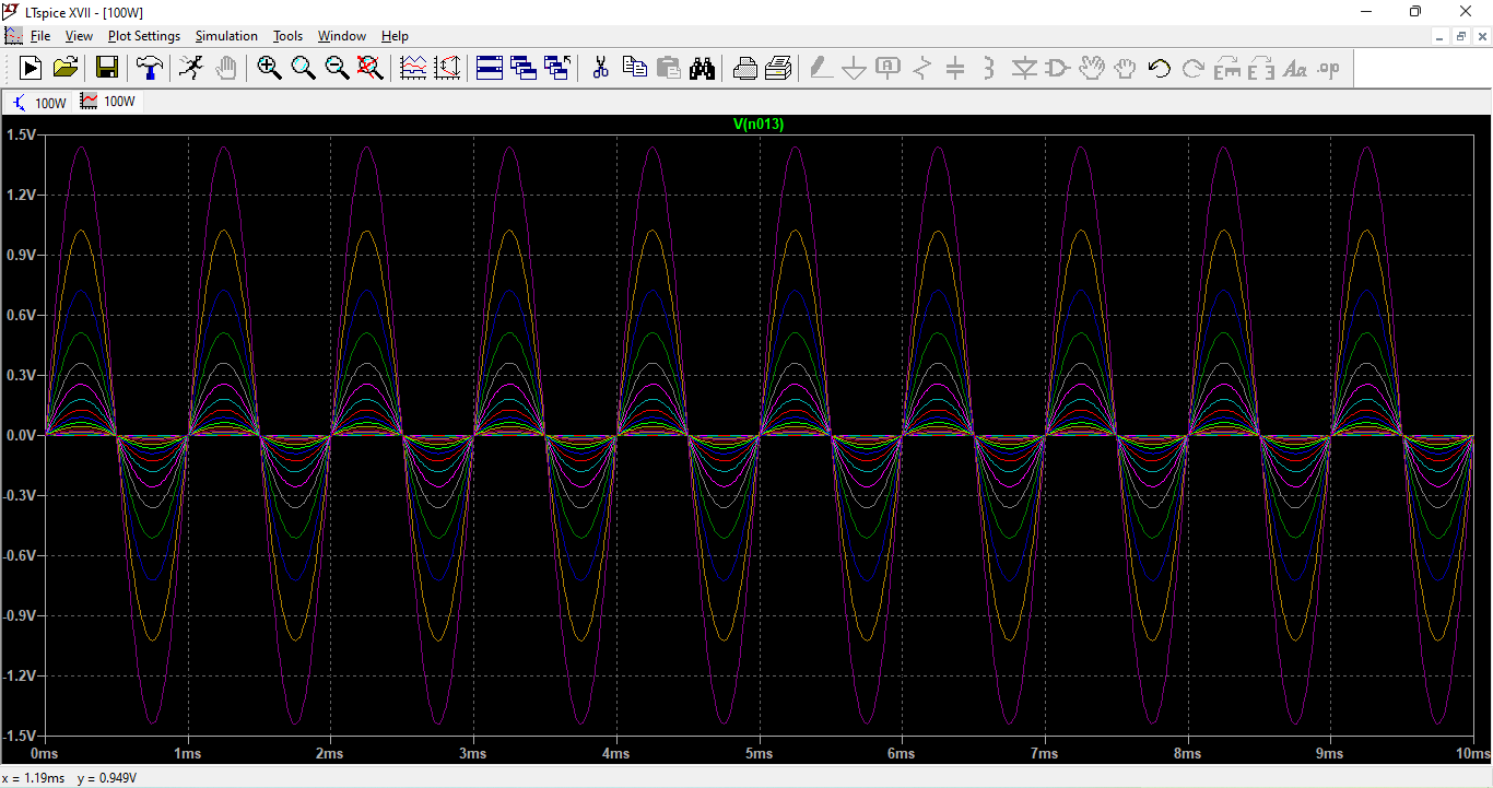
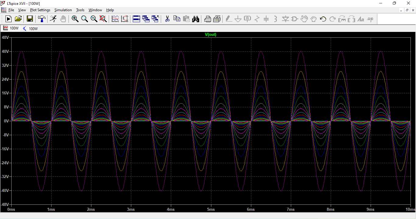
– Output Voltage: Stable 300Vpp achieved with both sine and square wave input
– Current: Measured peak current reached ~5.9A without thermal runaway
– Frequency Response: Clean response up to 1.8 MHz with minimal gain loss
– Stability: No oscillation or ringing observed within the bandwidth
– Efficiency: Overall power efficiency measured above 85% at 1MHz operation [5].
You can download the Project files here: Download files now. (You must be logged in).
4. Piezo Ultrasonic Transducer Integration
The amplifier was tested with a piezoelectric ultrasonic transducer operating at its resonant frequency (typically ~40kHz to 1MHz):
– Resonant Response: Transducer operated efficiently at resonance without signal degradation
– Impedance Matching: Additional series inductance was added for optimal energy transfer
– Long-term Stability: Continuous operation for 1 hour showed no thermal drift or frequency instability [7].
5. Operational Amplifier and Active Filters
Operational amplifier is also a building block, but a very sophisticated one, for electronics. An operational amplifier contains dozens of transistors. They are designed and integrated together to offer high performance. In this chapter, we discuss characteristics of operational amplifiers and learn how to design circuits using operational amplifiers.
Electronic amplifiers can boost weak signals. Basic characteristics of an amplifier include the gain or amplification factor, input impedance or loading to the signal source and output impedance or ability to drive the load. Operational amplifiers are nearly ideal. They offer a high input impedance, a large gain and a low output impedance. These characteristics greatly simplify the task of circuit design. They are much more convenient to use than discrete transistors [6].
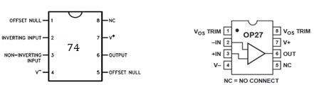
One of the following operational amplifiers, A741, OP27 or OP37, can be used to study characteristics of operational amplifiers. In the manufacturer’s datasheet, the following information can be found. As shown in Fig.1, pin 1 is next to the notch in a dual inline package (DIP) device. Pins are counted in the counter-clockwise direction. Pin 2 is the inverting input. Pin 3 is the non-inverting input. Pin 4 is the negative power supply. Pin 7 is the positive power supply. Pin 6 is the output. Pins 1 and 5 of 741 or pins 1 and 8 of OP27 are for offset adjustment. Pin 8 in 741 or pin 5 in OP27 is not connected. The maximum output voltage, i.e., the saturation voltage, is approximately 0.1 to 1 V below the power supply voltage. The power supply voltage can be 5 V to 15 V. The typical output short-circuit current is 40 mA. The typical slew rate, i.e., how fast the output voltage can change, is 0.5-2 V/sec.
Reader can find the circuit diagram inside of LM741 made by Texas Instrument. The file is located in LTspice XVIIexamplesEducation.
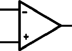
The symbol of an operational amplifier is shown in Fig. 2.
It has two input ports. One is the inverting input (V-IN), i.e., the output signal is 180o out of phase with respect to the signal at this input node. The other is the non-inverting input (V+IN). The open-loop gain, A, of a typical operational amplifier is large, i.e., >1000. It is internally compensated and short-circuit protected. It has an excellent stability, therefore, is free from any self-oscillation. For dc input, a dual voltage power supply with both positive and negative voltages should be used. The common node of the dual voltage power supply is connected to the circuit ground. For ac coupling, a single positive power supply is sufficient.
The output voltage, Vo, is related to the difference of voltages at the input.
𝑉𝑜 = 𝐴 ∙ (𝑉+𝐼𝑁 − 𝑉−𝐼𝑁). (1)
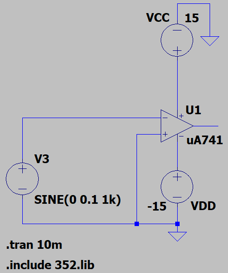
This is the differential gain. When two input voltages are the same, the common-mode gain is negligibly small. When there is no feedback loop from the output to the input, because of the large open-loop gain, a small input can drive the operational amplifier into saturation. A sine wave input can generate a square or trapezoidal wave at the output. Readers can simulate the circuit shown in Fig. 3 to find the saturation voltage. How far is the saturation voltage from the power supply voltage? (Answer: 0.5 V). In real devices, there may be a small difference between positive and negative saturation voltages.
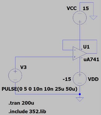
In additional to the limit on the maximum output voltage, there is also a limit on how fast the output voltage can change. The maximum rate of change is called the slew rate. To find the slew rate, readers can simulate the buffer amplifier with unity gain shown in Fig. 4. The input is a square wave. After running simulations, readers will find that the output is a trapezoidal signal. The slope of the rising edge and the trailing edge is finite. What is the slew rate? (Answer: 0.5 V/µsec).
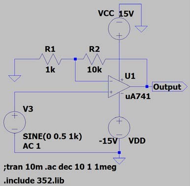
When a feedback resistor is connected from the output to the inverting input, the operational amplifier is intended for linear amplification. An example of a simple inverting amplifier is shown in Fig. 5. Since the input impedance of the operational amplifier is very large, any current provided by the signal source must flow through the feedback resistor, R2. In addition, the open-loop gain is very large. Therefore, the voltage difference between two input ports must be nearly zero. Since the non-inverting input is connected to the ground, the inverting input port is virtually grounded. From the current flow, one can easily find the voltage gain, which is the ratio of the output voltage to that of the input voltage provided by the waveform generator, Vo/Vin.
𝐴𝑣 = −𝑅2/𝑅1. (2)
You can download the Project files here: Download files now. (You must be logged in).
The negative sign simply indicates that there is a 180o phase shift between the input and output signals. A positive input voltage is amplified to become a negative output voltage.
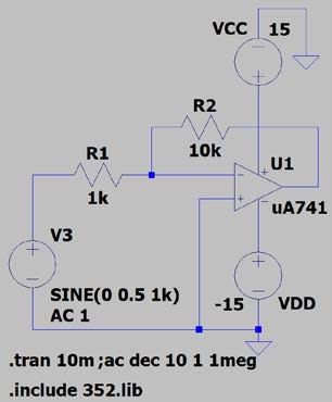
The input impedance of an operational amplifier is large but not infinite. The output impedance is low but non-zero. Therefore, resistors in the range of k to a few hundred k should be used in constructing the amplifier circuit. Otherwise, assumptions used in deriving the voltage gain become invalid. What is the gain for the circuit shown in Fig. 5? (Answer: -10). Perform the ac analysis to obtain the Bode plot, i.e., the frequency response. What is the -3 dB frequency? (Answer: 72 kHz). By changing R2 to 100 kΩ what is the gain? (-100). What is the -3 dB frequency for a gain of -100? (Answer: 10 kHz). This is another example that the higher the gain, the lower is the high-frequency cutoff.
Operational amplifiers do deviate from the ideal amplifier. At the input, there are input offset, common-mode input resistance, differential input resistance and input bias current. At the output, there is the current driving capability. The open-loop differential gain, A, is large but finite. It also drops off as the frequency is increased. The common-mode gain is small but not exactly zero. The current driving capability can be found in simulations. Attach a 100-kΩ load resistor to the operational amplifier circuit shown in Fig. 5. Reduce the load resistance until the tip of the sine wave output starts to clip. The amplitude of the clipped output signal divided by the load resistance is the current driving capability. What is the current driving capability of 741? (Answer: 40 mA). The common-mode gain of this circuit can also be found in simulations. Rewire the non-inverting input. Connect it to the inverting input. When the input amplitude is 0.1 V, what is the output peak-to-peak voltage? (Answer: 6 mV). The ratio between the differential mode gain and the common- mode gain is the common-mode rejection ratio. In real devices, there may still be an output when the differential input is zero. This offset can be nulled by connecting two end pins of a potentiometer to the offset adjustment pins of the operational amplifier. Connect the center wiper pin to the negative power supply. Adjust the potentiometer until the output offset is zero.
An operational amplifier can also be configured to amplify without a phase reversal. The circuit diagram is shown in Fig. 6. The input is connected to the non-inverting input. Using the virtual ground concept, one can derive the voltage gain as:
𝐴𝑣 = (𝑅1 + 𝑅2)/𝑅1. (3)
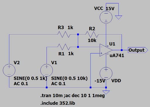
Furthermore, an operational amplifier can perform the addition of two or more signals. The diagram of a summing amplifier is shown in Fig. 7. There are two input signals. Each voltage source generates a current. The total current flowing through R2 generates the output signal. The output signal is proportional to the sum of two input signals but with a negative sign. Run the simulation. Display the two input waveforms and the output waveform. Can you design an operational amplifier circuit to perform the subtraction of two input signals?
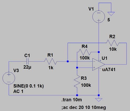
Many operational amplifiers can work with only a single power supply. However, a dc reference at half the power supply voltage and ac coupling through a capacitor are needed. The circuit diagram is shown in Fig. 8. The dc reference can be obtained from a simple voltage divider. At the input, R1 and C1 form a high-pass filter circuit. There is a low-frequency cutoff.
You can download the Project files here: Download files now. (You must be logged in).
The power supply voltage can be as low as +5 V. Filters are widely used in electronics. They can control the bandwidth, hence, reject noise outside of the signal band. Using operational amplifiers, one can design active filters. Active filters can provide a gain, drive the load, and facilitate sophisticated high-order filters with sharp frequency responses and high Q values. There are active low-pass, high- pass, band-pass, notch and band-reject filters. Texas Instruments (TI), a manufacturer of operational amplifiers and other electronic components, provides application notes and design references for operation amplifiers. Chapter 16 in “Op Amps for Everyone,” Ron Mancini, Editor in Chief, SLOD006B, August 2002 is dedicated to the active filter design. Readers can also find “Filter Design in Thirty Seconds,” Bruce Carter, SLOA093, December 2001 on TI website: https://www.ti.com/lit/an/sloa093/sloa093.pdf. In it, you can find circuit diagrams and design procedures for essentially all types of active filters.
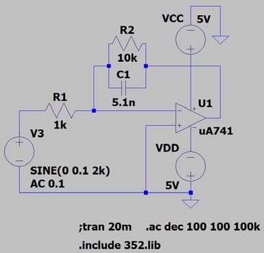
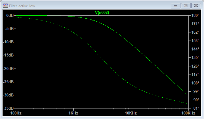
For comparison, two low-pass active filters are presented below. The circuit diagram of the first-order, low-pass active filter is shown in Fig. 9. In the circuit, R1 and C1 form an integrator. To cap the gain at dc, R2 is incorporated in the feedback loop.
Its Bode plot is shown in Fig. 10.
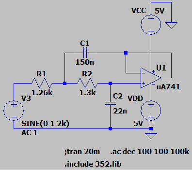
The circuit diagram of a second-order low-pass active filter is shown in Fig. 11.
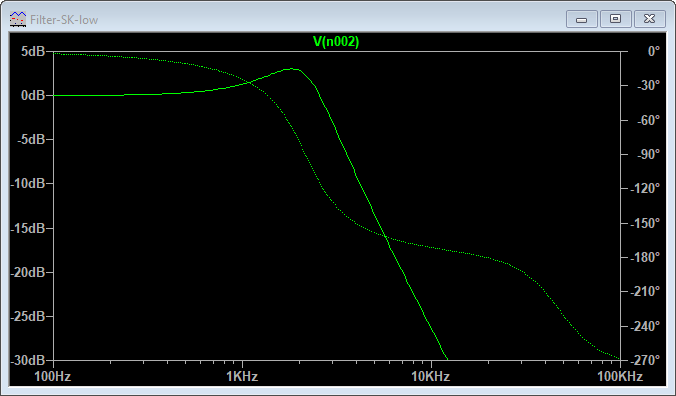
The second-order active filter has a much sharper roll off beyond 3 kHz. It also has a ripple in the pass band. By cascading the first and second order filters, one can obtain third and higher order filters.
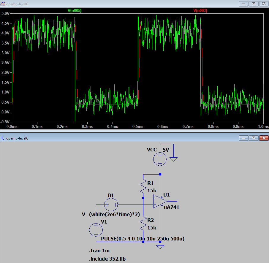
The use of operational amplifiers extends into the digital realm. When noise is present, a decision circuit is needed to quantize the signal into either logic H or L. The level comparator circuit shown in Fig. 13 is an example. In this example, the decision level is set at half of the power supply voltage. The input signal shown in green contains a significant amount noise. When the input is above 2.5 V, the output is H. When the input is below 2.5 V, the output is L. The output signal shown in red is noise free.
You can download the Project files here: Download files now. (You must be logged in).
6. Conclusion
In this chapter, we learn the basic characteristics, such as the saturation voltage, slew rate and current driving capability, of an operational amplifier. We learn how to build amplifiers and the gain-bandwidth correlation. We also learn how to build active filters and the level comparator.
The project successfully demonstrated the design, simulation, prototyping, and real-world validation of a power amplifier tailored for ultrasonic transducers. Using LTSpice simulations and Altium PCB design, the amplifier was optimized to handle high-voltage outputs across a 25Ω load with excellent efficiency and stability.
The amplifier met all target specifications:
– 300Vpp output
– Up to 6A peak current
– Stable response across 1kHz to 2MHz
– Efficient integration with piezo transducers
This system provides a robust foundation for future work in medical imaging, industrial ultrasonic processing, and high-frequency actuation systems.
References
[1] Sedra, A. S., & Smith, K. C. (2015). Microelectronic Circuits (7th ed.). Oxford University Press.
[2] Rashid, M. H. (2017). Power Electronics: Circuits, Devices and Applications (4th ed.). Pearson.
[3] The AnyLogic Company. (2022). AnyLogic Simulation Software. Available: https://www.anylogic.com
[4] LTSpice Documentation. (2022). Analog Devices. Available: https://www.analog.com/en/design-center/design-tools-and-calculators/ltspice-simulator.html
[5] IRFP460 Datasheet. Infineon Technologies AG.
[6] IR2110 Gate Driver Datasheet. International Rectifier.
[7] IPC-2221: Generic Standard on Printed Board Design. IPC International Inc.
You can download the Project files here: Download files now. (You must be logged in).
Keywords: Power Amplifier Design, LTSpice, Altium, Piezo Ultrasonic Transducers, Circuit design, Electronics circuit


Responses