

A Comparative Analysis of an XOR-XOR Based 18-Transistor Full Adder Cell in LTSpice

Author: Waqas Javaid
Abstract
This research presents a comparative study between a novel XOR-XOR based 18-transistor full adder cell and a standard fully complementary CMOS-based full adder. The primary objective is to evaluate and contrast the performance of both architectures in terms of propagation delay and power dissipation. Simulations were conducted in LTSpice using BS170 (nMOS) and BS250 (pMOS) transistors to mirror realistic device behavior. Sixteen different logical input combinations were used to test both circuits, and the timing and power characteristics were extracted through dedicated LTSpice commands. Results indicate that the CMOS-based design outperforms the XOR-XOR based architecture in both delay and energy metrics. Notably, the reduced performance of the proposed full adder is largely attributed to the pull-down resistors introduced during its design modifications. Nonetheless, the XOR-XOR architecture provides important insights into compact design strategies that can be optimized further.
Introduction
Adders are fundamental building blocks in digital systems such as arithmetic logic units (ALUs), digital signal processors (DSPs), and microprocessors. Their efficiency significantly influences the overall performance, power consumption, and area of integrated circuits. A full adder circuit computes the sum of three binary inputs (A, B, and Cin) and generates sum and carry outputs. Traditional implementations use complementary CMOS logic, which is known for robustness and low power leakage but tends to consume more transistors and silicon area [1].
Recent research efforts have focused on minimizing the transistor count while maintaining functional integrity and acceptable performance levels. One such approach is the XOR-XOR based full adder design, which utilizes XOR gates at the core of its logic to achieve compactness. The proposed 18-transistor full adder aims to reduce complexity and increase design efficiency [2]. However, transistor reduction may lead to trade-offs in performance, especially in terms of delay and power dissipation due to altered switching characteristics.
This report evaluates and compares both architectures through simulation in LTSpice, offering insights into how design decisions affect key performance metrics. The research further explores the influence of supporting components, such as pull-down resistors, on the behavior of the XOR-XOR architecture.
Circuit Design Description
The XOR-XOR based 18-transistor full adder uses a combination of two XOR gates followed by logic elements for carry generation. The XOR gates are constructed using minimum transistor count techniques, prioritizing area efficiency. Meanwhile, the standard CMOS full adder design implements NAND, NOR, and inverter logic structures, using a complementary arrangement of pMOS and nMOS transistors to ensure low static power and high noise margins [3].
In both cases, the designs were simulated under identical conditions. The supply voltage was set to 5 V, with inputs toggled for all 16 logical combinations. Transistor parameters were defined using BS170 and BS250 models, providing a consistent basis for comparison.
Simulation Setup in LTSpice
LTSpice XVII was used as the simulation platform. The XOR-XOR and CMOS full adder circuits were modeled and tested using standard transient analysis. Timing and power measurements were obtained using voltage and current probes combined with behavioral SPICE commands. LTSpice commands were written to automatically measure:
- Propagation delays (rise and fall)
- Average power consumption over simulation time
Each of the 16 input combinations was simulated for both designs. The XOR-XOR design included pull-down resistors to ensure proper output logic levels, particularly for low-strength signals.
Automata description of a FTJ_Cell in LTSpice
The automata of the behaviour of a FTJ cell is modelled by the .machine statement, which was newly introduced in LTS pice Version XVII. It allows to model and to simulate finite state machines or finite automata in S PICE netlists.
The general syntax for the description of an automata is as follows:
.mach[ine] [] ; tripdt is an optional temporal tolerance
.state
.rule
.output (node)
.endmach[ine] ; end of block
The meaning of that tripdt option is not clear to me currently. By opportunity, I will try to find it out. For our investigations of modelling FTJ cells it is not essential at first.
The .state command allows to define different states, which can be assigned to an initial value . If this is made value can be used later in an arithmetic expression that is evaluated to determine a value that is given out later with the .output command [4].
The .rule command allows to define a state transfer from the state defined in to the next state , which will occur if the condition formulated in is fulfilled. This new state will be then the current state of the automata. This value can be accessed in an arbitrary S PICE netlist via the node
. The .rule * command is to interpret as follows. From any arbitrary state a transfer to the state will happen, if the condition formulated in
is fulfilled.
The .output(node) command defines the output(s) of the defined automata. Either the value assigned to the current state is given out, e.g. with the command
.output (1)state, that value is given out at node node, that was initially defined for that state, which is the current state. E.g., look to the example shown below. If the current state is the state S1b the value ‘1’will be given out at node 4.
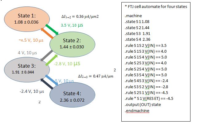
The following figure shows Suzanne’s automata model for an FTJ cell, specified with an LTS pice compatible .machine command. In addition the LTSpice model contains already state transfers that go over the next direct state neighbour, e.g. directly from state S 1 to state S 3, or from state S 1 to S 4.
∆𝐼3→4 = 0.45 𝑝𝐴/µ𝑚
Simulation of an FTJ cell as automata in LTSpice
In the screenshot of the schematic editor shown figure 1 we define a simulation environment for the FTJ cell modelled as automata. The FTJ cell has four input stimuli, IN,RESET, READ, and WRITE, and one output stimuli OUT1. The input signal IN corresponds to an input sequence of voltages in order to program the FTJ cell under stimulation in the single states from S 1 to S 4 and back subsequently. The input signal RESET is used in order to switch the FTJ cell to the initial state S 1 at the beginning of the simulation. The input signal READ is a voltage corresponding to the read out voltage of 1.5 V. For a better synchronization and distinguishing of read and write phase, an explicit control signal WRITE for the writing procedure was defined.
A writing of a state is only possible if V(WRITE)is equal to 5 V, which is to see in each of the defined rules for a state transfer, e.g. for a state transition from S 1 to S 2 the following command is to use.
rule S1 S2 (((3.51 > V(IN) & (V(IN) > 3.49)) & (V(WRITE) == 5.0))
Furthermore, a tolerance region of 0.01 V is defined for the required input voltage of 3.5 V, which is necessary to cause a state transfer from S 1 to S 2. Corresponding rules are defined for the other state transitions.
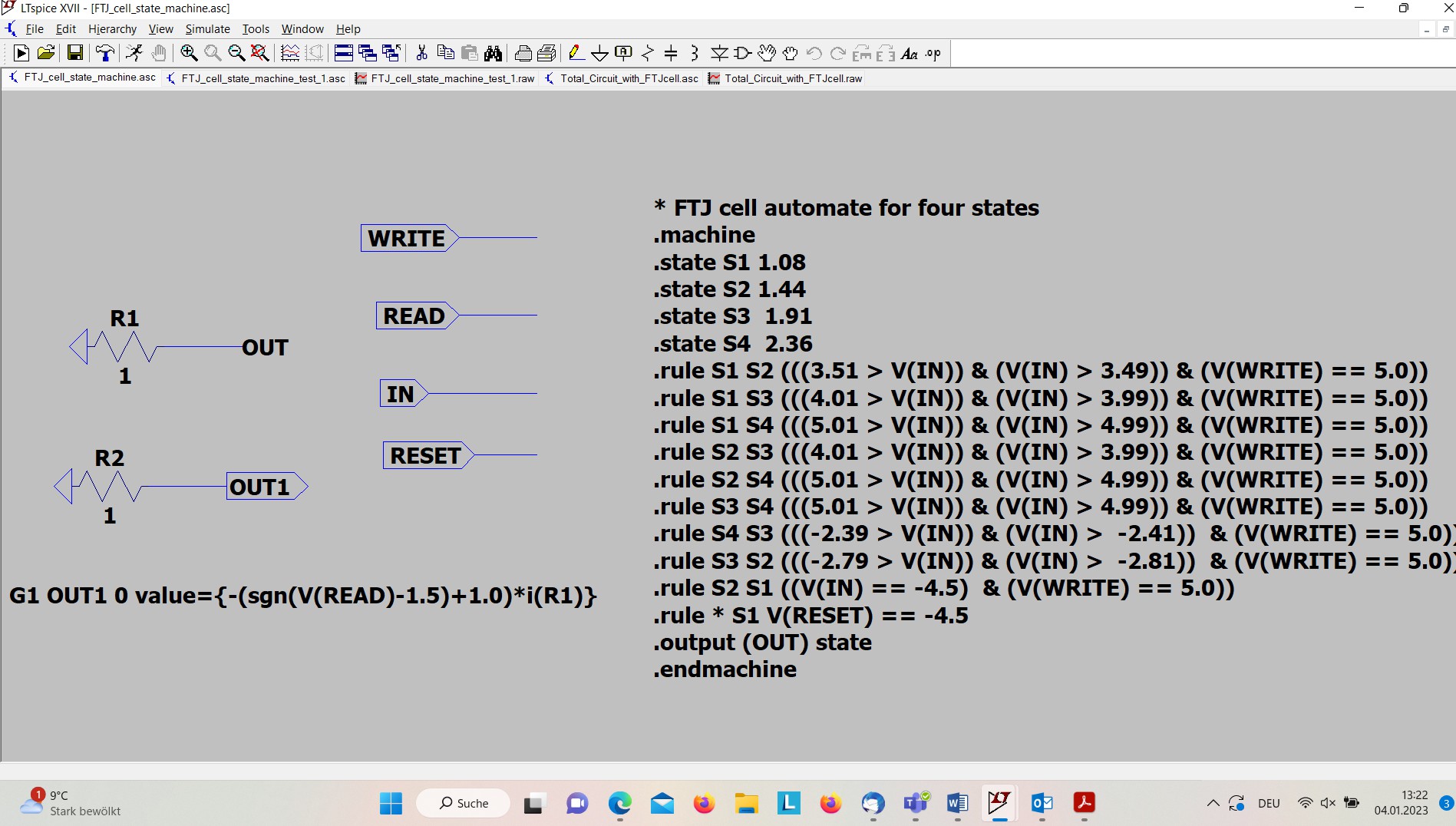
For reading out the stored resistivity, resp. the current state, the output of the automata is attached to an output node called OUT. To get out the current a modelling “trick” had to be applied by attaching the node OUT to a resistor R1 with a resistance of 1 Ohm. Therefore, the current flowing through R1 corresponds directly to the values, assigned to the single states, namely 1.08 A (ampere) to S 1, 1.44 A to S 2, 1.91 A to S 3, and 2.36 A to S 4. The current running through R1, i(R1), is coupled with a voltage controlled current source G1 to the output node OUT1,(G1 OUT1 0 value=…). This has to be done in that indirect way because an output node of an automata, in the example OUT, cannot be used as pin interface in a hierarchical design, what we want to do later, if the FTJ cell will be part of a larger circuit. Again the output pin OUT1 is attached to a resistor of 1 Ohm to read out the voltage and the current flowing to that pin. In order to produce an output value, if and only if the read voltage READ is equal to 1.5 V, we use the expression sgn(V(READ)- 1.5)+1.0. This expression is exactly 1, if V(READ)=1.5, and it is 0 if V(READ)is < 1.5 V.
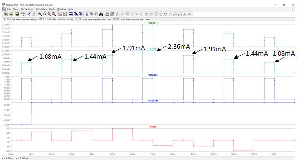
The next figure 2 shows the plot of the simulation run. We detect clearly the RESET of the FTJ cell by an applied voltage V(reset)= -4.5 V during the first 1 ms. A read out of the cell is already started at 0.5 ms with V(read) = 1.5 V, leading to the expected output current I(R1)= 1.08 mA. A at o state S1, which corresponds exactly to an output current of 1.08 µA after reading out the cell with V(READ)= 1.5 V at time 0.5 ms. With the next steps V(in)is set to 3.5 V, 4 V, 5 V and the output current I(R1) increases to the corresponding values 1.44 mA, 1.91 mA, and 2.36 mA. Finally the switching process happens in reverse order by applying subsequently -2.4 V, -2.8 V and -4.5 V setting the state of the cFTJ cell subsequently to S 3, S2, and S 1, what can be verified by the corresponding output currents. For reasons of completeness the corresponding output voltages are also shown in the wave diagram. The necessary setting of the write signal V(WRITE)to start the write phase is not shown in the wave diagram but it was applied at the right time points [5].
Next we want to simulate an in LTSpice generated macro cell of the FTJ cell, denoted as
FTJ_Cell_1 (see figure 3). By using a macro cell we can use FTJ cells in more complex hierarchical designs. We simulate this new arrangement with the same stimuli as before in the plain design to verify that our macro cell works correctly.
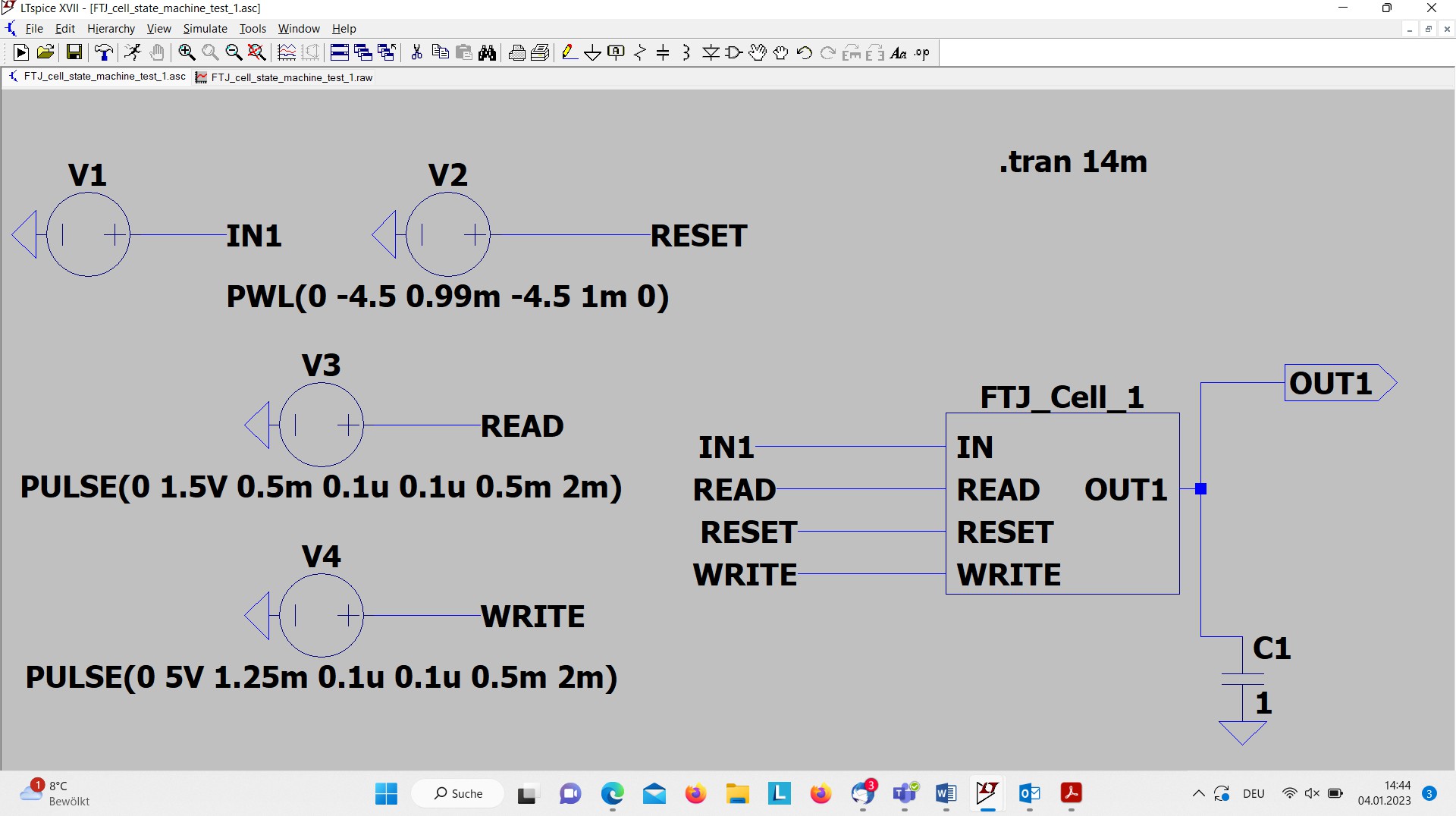
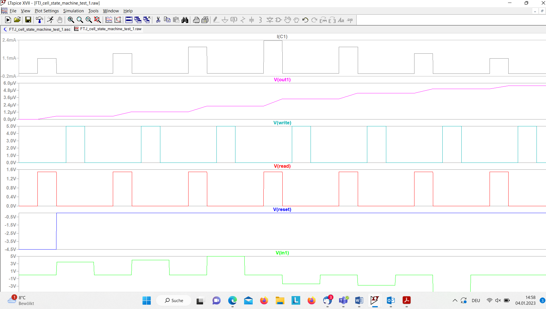
The schematic contains the FTJ_Cell in the right center, with its three input interfaces IN, RESET, and READ and the output pin OUT1. The input voltage RESET is defined as piece wise linear (PWL) function, that starts at 0 ms with -4.5 Volt, this level is kept up to .99ms and then jumps back to 0 Volt at 1 ms. This “trick” of an increase from -4.5 V to 0 V within 0.01 ms is used in order to generate a sharp pulse transition at 1 ms in the linear interpolation of the PWL representation. The task of this pulse form is to reset the FTJ_Cell to state S1 at the beginning of the simulation. The input voltage V1, applied to the input pin IN via the interface IN1 is used to apply the corresponding voltage levels to switch the FTJ_Cell from one state to the next one. The pulse sequence of 3 V, 4 V, 5 V, -2.4 V, -2.8 V, -4.5V is not shown on the schematic. The third input voltage READ is defined as periodic pulse (PULSE(0 1.5V 0.5m 0.1u 0.1u 0.5m 2m)) that increases from 0 V to the read out voltage 1.5 V, a rise and fall time of 0.1 µs, a high and low level phase length of 0.5 ms, and a period length of 2 ms. The output current of the FTJ cell is used to be collected at the capacity C1 and can be directly measured by using a value of 1F for C1.
The waveform viewer in figure 4 shows the result of the simulation run. Always when the read voltage V(READ is active, i.e. 1.5 V, the previous programmed states via a corresponding pulse IN of appropriate amount is read out. Clear to detect is the increase and subsequent decrease of the amplitudes of the output current I(C1) at each READ pulse and the at the capacity C1 accumulated voltage at V(out)node OUT, corresponding to the subsequently programmed states S1, S2, S3, S4, S3, S2, and S1.
You can download the Project files here: Download files now. (You must be logged in).
Processing of the ternary inputs with digital logic and interfacing to FTJ cell
The following table is an example for an addition of two ternary signed-digit (SD) numbers, X and Y, in two steps. In the first step the ternary number X is added with the negative channel of the ternary operand Y. In Y each ternary digit y is coded by two digital coded bits (y+,y–) in a so-called plus/minus coding, i.e. the first entry of the code vector is interpreted positively, the second entry is to interpret negatively, i.e. (1,1) and (0,0) correspond to the ternary digit (trit) 0, (1,0) corresponds to the trit 1, and (0,1) corresponds to the trit -1 = 1�.
| X | 1 | 1� | 0 | 1� | 0 | 1 | 0 | 1� | ||
| Y– | + | 0 | 1� | 0 | 1� | 0 | 0 | 0 | 0 | |
| s+ | 1 | 0 | 0 | 0 | 0 | 1 | 0 | 1 | ||
| c– | 0 | 1� | 0 | 1� | 0 | 0 | 0 | 1� | 0 | |
| M | 0 | 0 | 0 | 1� | 0 | 0 | 1 | 1� | 1 | |
| Y+ | + | 0 | 1 | 0 | 1 | 0 | 0 | 0 | 1 | 0 |
| s– | 0 | 1� | 0 | 0 | 0 | 0 | 1� | 0 | 1� | |
| c+ | 0 | 1 | 0 | 0 | 0 | 0 | 1 | 0 | 1 | 0 |
| sum | 1 | 1� | 0 | 0 | 0 | 0 | 1� | 1 | 1� |
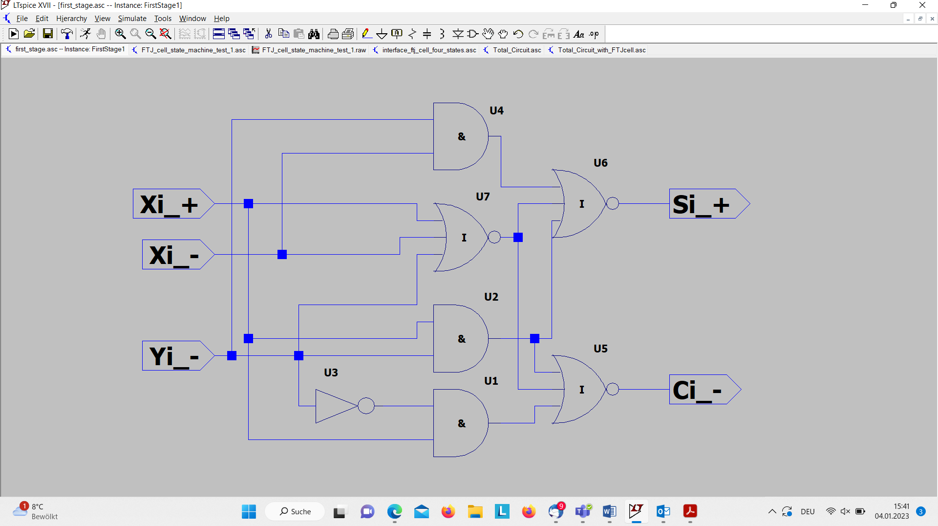
The following figure 5 shows the complete circuit for four digits. The component FirstStagei (1<= i <= 4) generates with a corresponding Boolean circuit the outputs s + and c –.
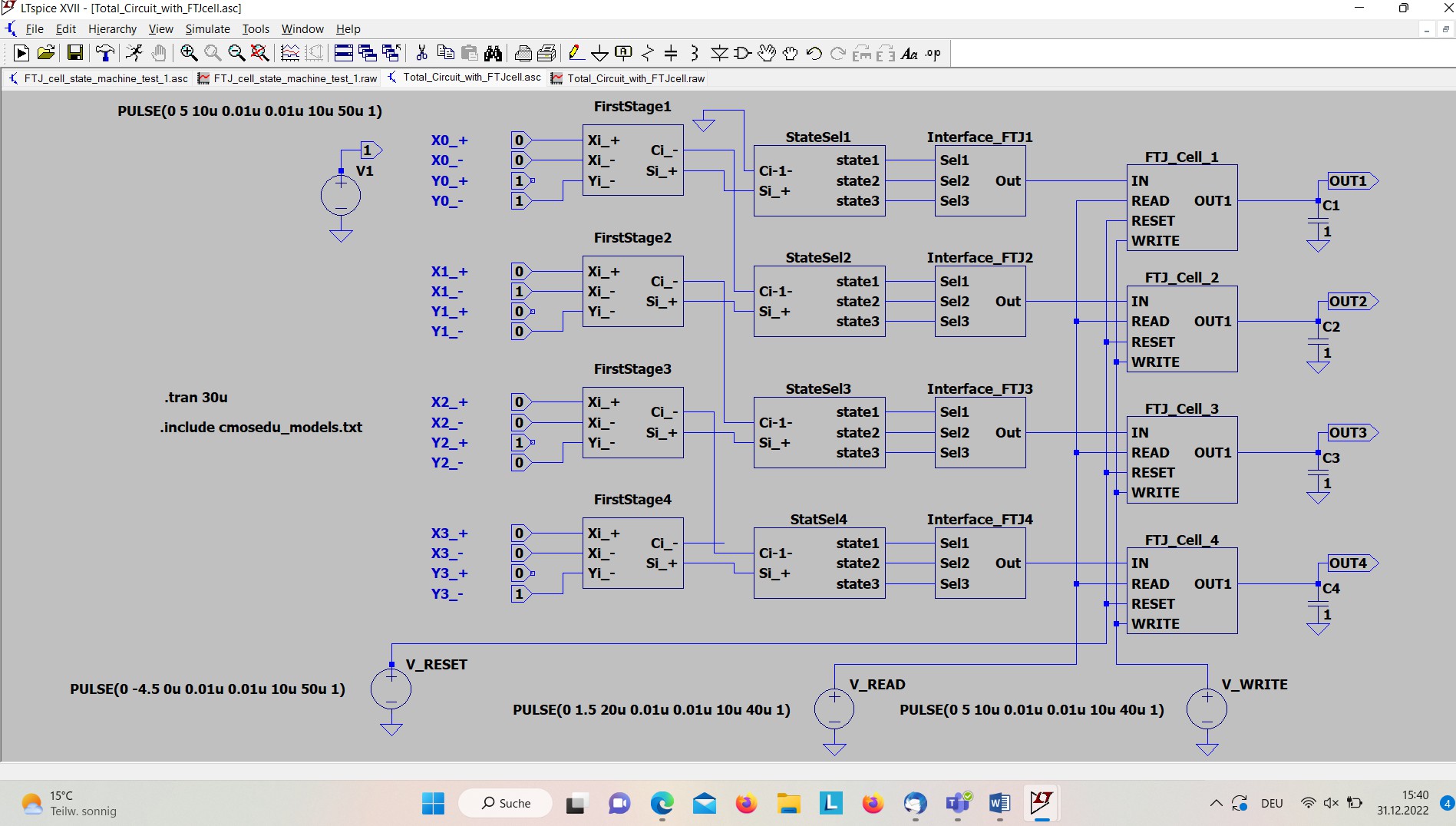
Figure 6 shows the inner Boolean circuit of the component FirstStage1. Its logic is based completely on digital logic gates for which a LTSpice library cmosedu_models.txt is used [6].
As we can see in figure 5 the component FirstStage is followed by a component StateSel. Task of that component is to determine which state has to be stored in the FTJ cell. According to its inputs s + and c – the component StateSeli (Figure 7 shows the interior by a schematic) generates in one of its three outputs state1 to state3 exactly about 1 V for the state that is to store in the FTJ_cell and which is coded as follows (M = -1 → state1, M =0 → state1, M = +1 → state2). The 1V output is produced by a 5:1 voltage divider since the used CMOS gates generate 5V outputs.
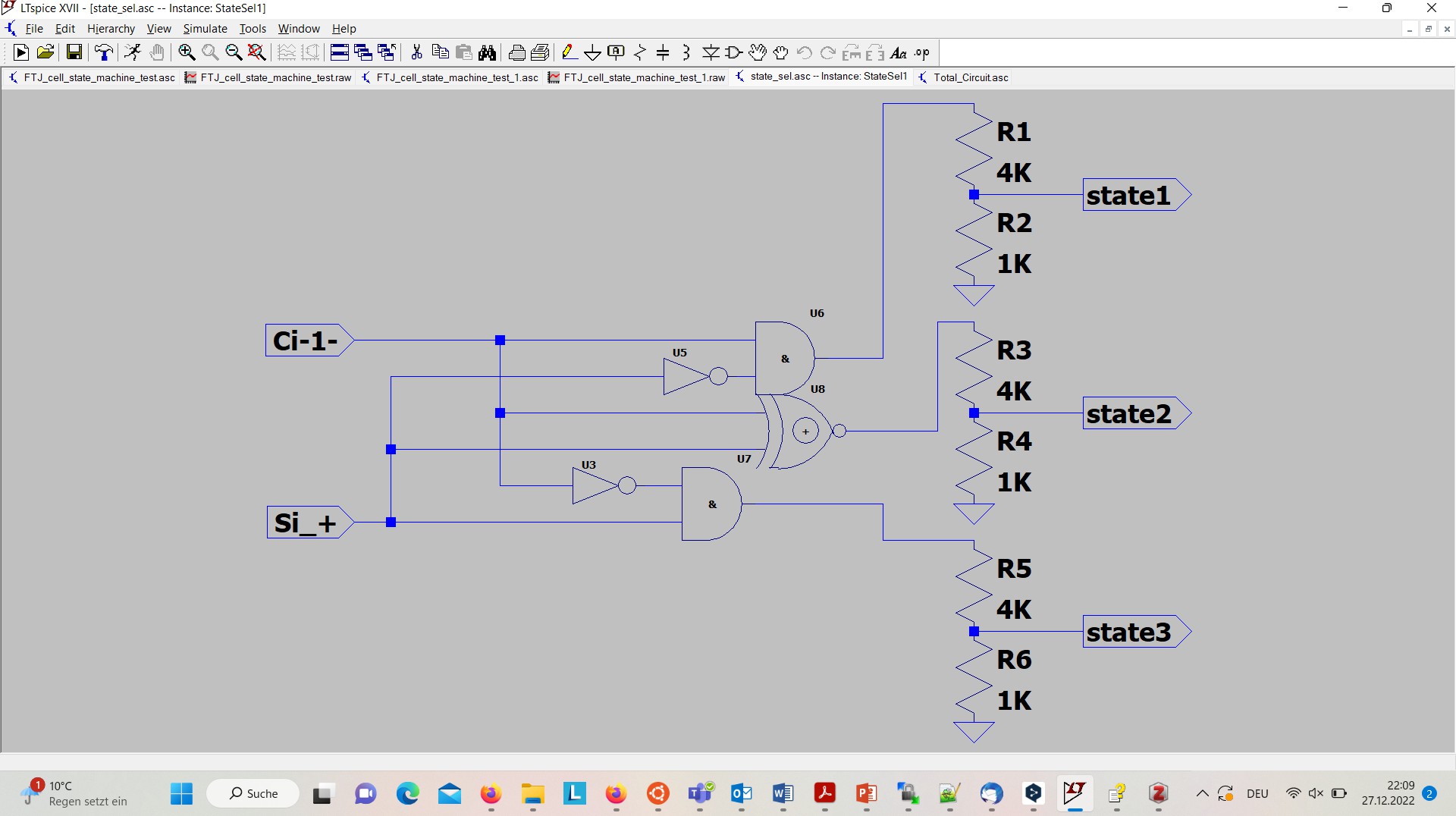
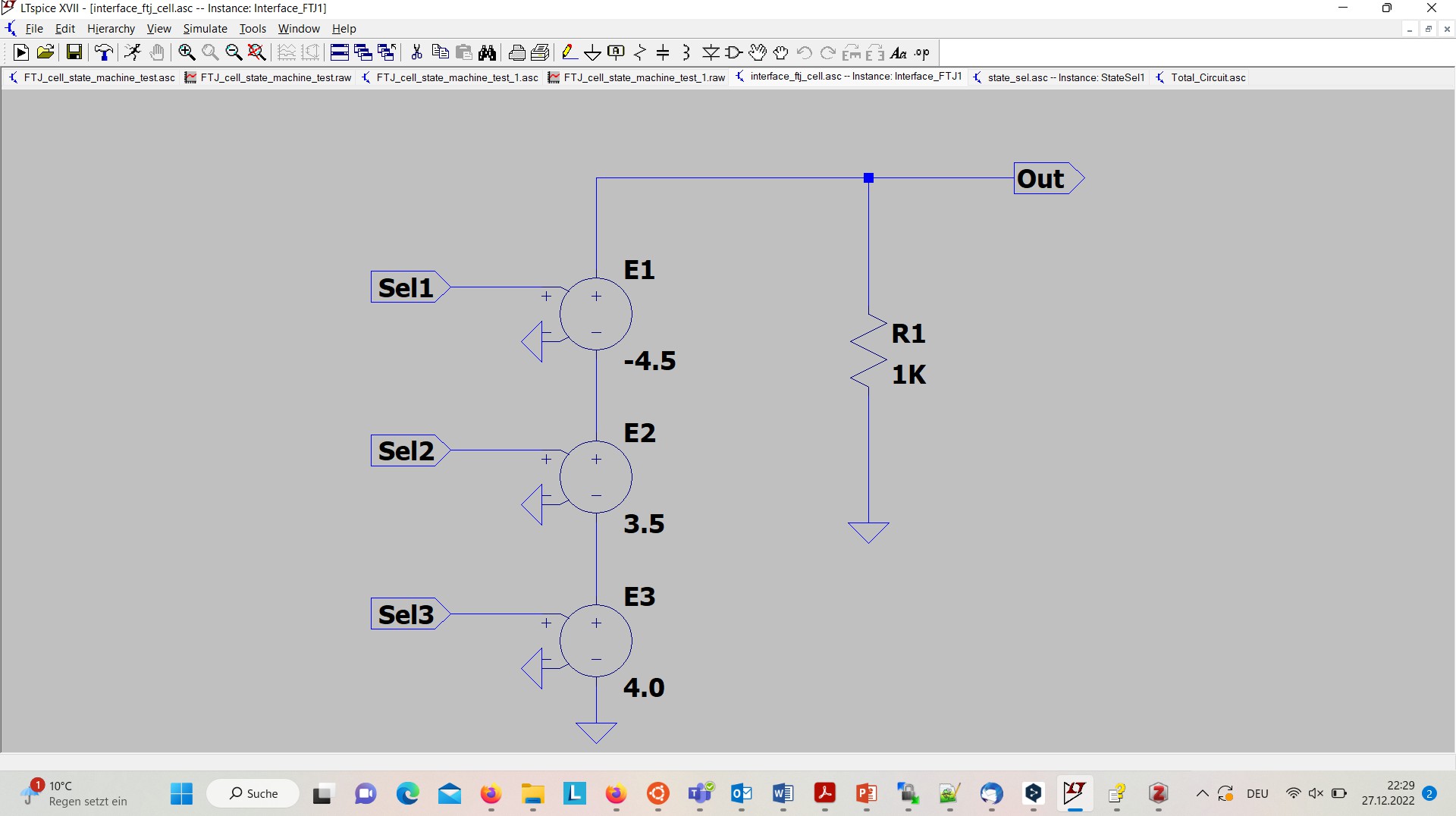
To the output side of the StateSeli components are attached the component Interface_FTJi whose task is it to provide the right programming voltage for storing the desired state in the FTJ cell. The interior of that component is shown in figure 8. The component has three input interfaces, Sel1 to Sel3, and one output interface, Out, where the corresponding programming voltage is given out. Exactly one of the three inputs Sel1 to Sel3 of the component is ~ 1V, the other two ones are 0V [7].
For the generation of the programming voltage of the FTJ_cells voltage dependant voltage sources E1 to E3 are used, in which the input voltage, namely 1V, is multiplied with the specified value, e.g. -4.5 in E1, 3.5 in E2, and 4.0 in E3. That produces exactly the desired programming voltage, either -4.5 V, 3.5 V or 4.0 V at the output interface Out. To be able to measure the output voltage in LTSpice a terminating resistor R1 of 1 Ohm has to be connect in parallel to the series of voltage dependant voltage sources.
The following wave diagram in figure 9 shows the simulation output of the complete circuit of figure 5 that stores the result after the first step of the ternary addition in its four FTJ cells FTJ_cell_1 to FTJ_Cell_4. According to the ternary inputs corresponding programming voltages are generated at the output out of the interface components Interface_FTJi, which are the inputs for the port IN at the FTJ cells FTJ_Cell_i.
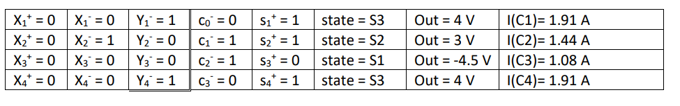
The following table lists the output currents I(Ci) to expect for the four digit positions i:(1 <= i <= 4) for the ternary inputs X +, X –, and Y – and the intermediate results c – and s +, the corresponding states and output voltages (not shown in the wave diagram).
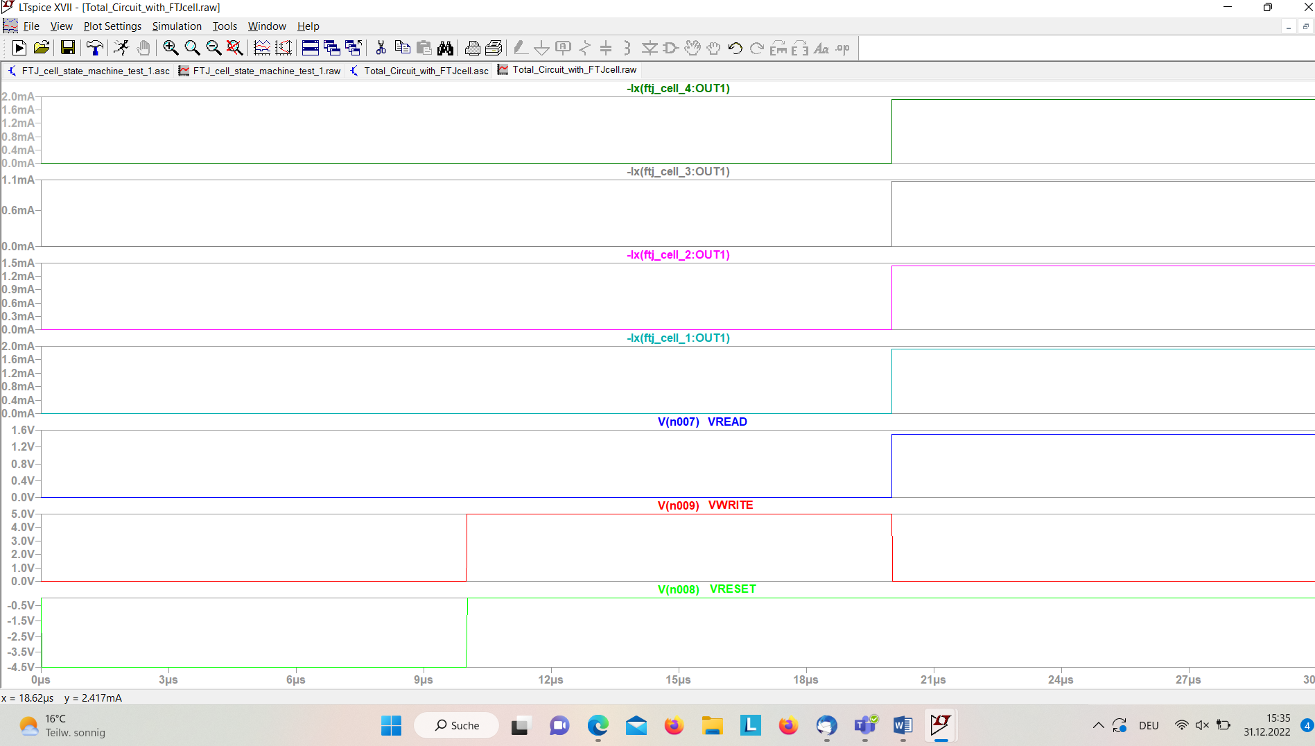
The wave diagram of the simulation proves the functionality. After the active phase of the RESET signal (VRESET = -4.5 V for the first 10µs) at the beginning all states of the FTJ_Cells are set to state S1. During the active phase of the signal VWRITE = 5 V (between 10 and 20 µs) the states in the FTJ_cells are programmed according to the input voltages V(IN), which are determined by the ternary input signals and the sequence of the components FirstStage, StateSel and Interface_FTJ as shown above. According to the inputs corresponding states are programmed and corresponding output currents ftj_cell_i(OUT1)= I(Ci) are measured [8].
The corresponding result currents of the four FTJ_Cells Ix(ftj_cell_i:OUT1), 1 <= i <= 4, represent the desired outputs for the stored three different states S3, S2, S1, and S3 in the four cells (see table above).
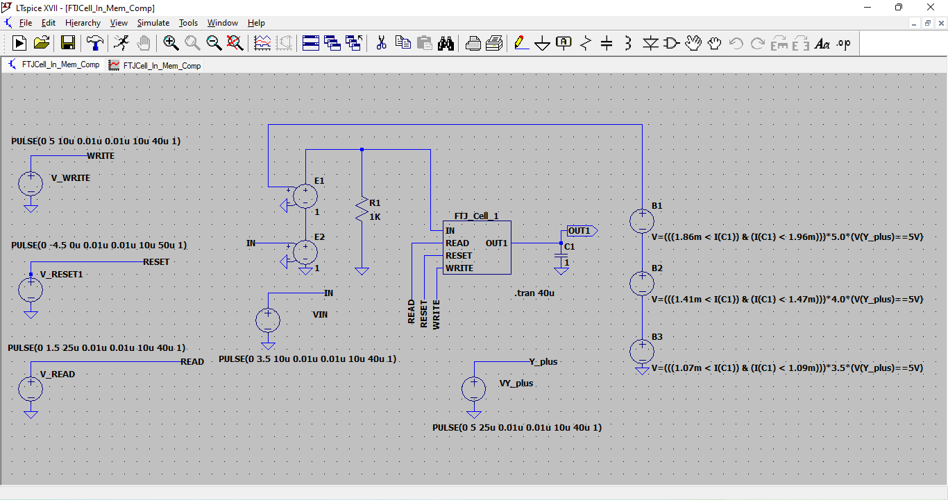
I) Testing FTJ_Cell in an In_Memory_Computing operation
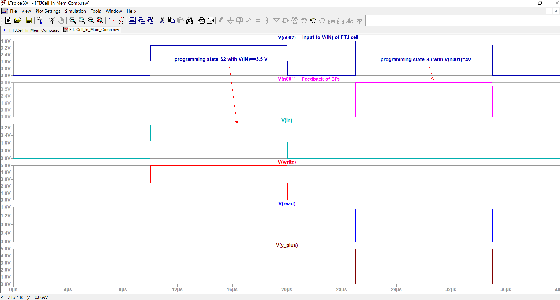
The following schematic shown in figure 10 gives an example for using an FTJ_cell in a kind of in- memory computing application. Here the shown cell FTJ_cell_1 is first reset by V_RESET1 and later triggered by V_WRITE and programmed by VIN = 3.5 V to state S1.
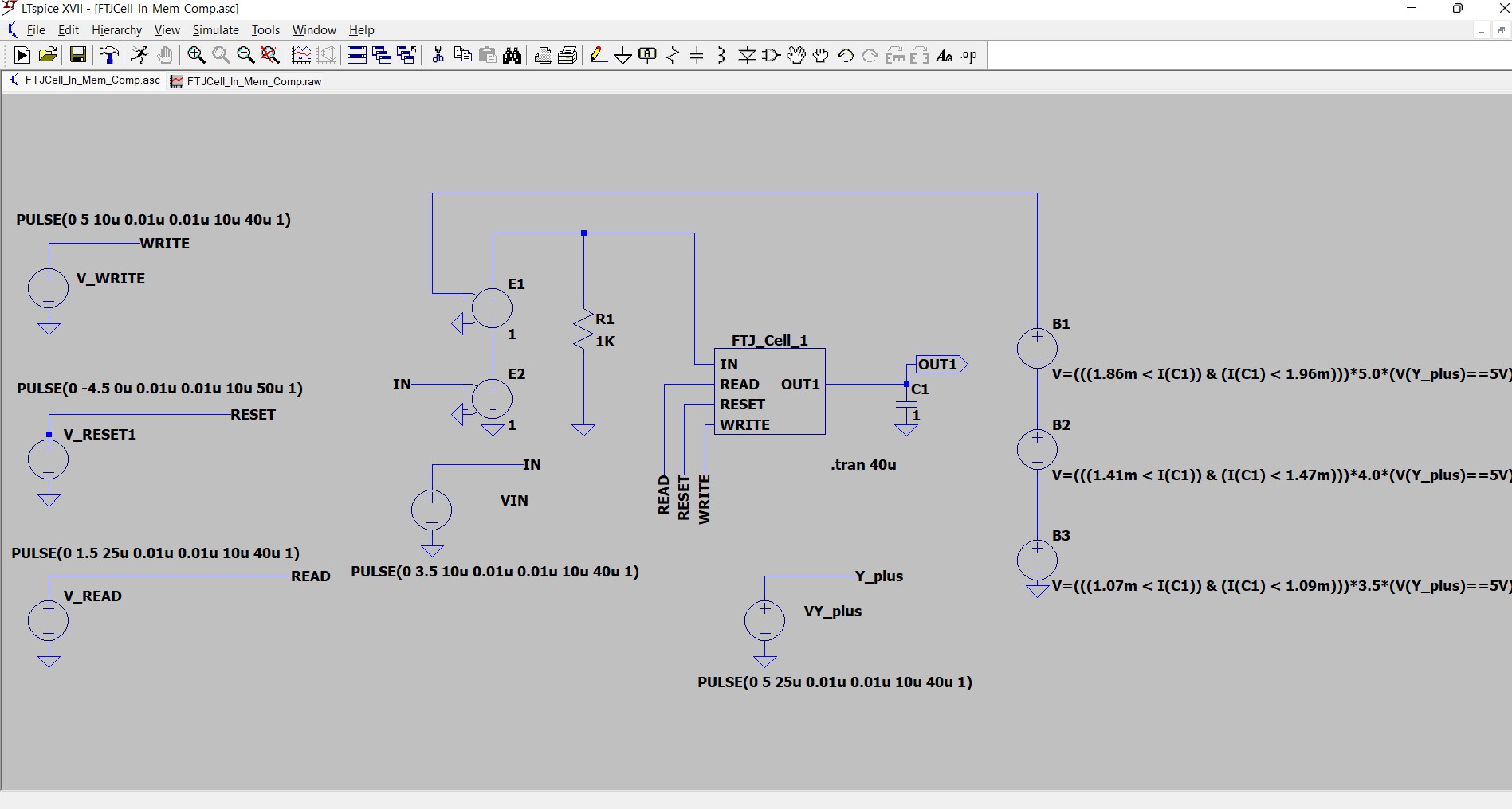
Again as before, the state of the FTJ cell can be read out, if V_READ is equal to 1.5 V. The read out current is measured by the current that loads the capacity C1,which has 1 Farad so that the constant load current I(C1) corresponds directly to the current assigned to a certain state of the FTJ cell. According to the amount of that current three so-call behavioural voltage sources B1 to B3 are used to produce a new programming voltage for the FTJ cell. These behavioural sources evaluate a condition, e.g. B1 (1.86m < I(C1) & (I(C1) < 1.96m), i.e. if the read out current is between the range of 1.86 mA to 1.96 mA, concerning to state S3, and the input voltage V(Y_plus)is equal to 5V, i.e. the ternary digit of the operand is +1, an output programming voltage of 5V is produced. This means, the FTJ_cell is switched from S3 to S4. The other two behavioural sources B2 and B3 realize the transfer from S1 to S2, resp., from S2 to S3, corresponding to the addition of a ternary 1.
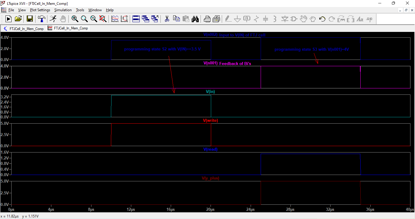
The following figure 11 shows the result of the corresponding simulation. The first given input voltage V(IN) and the feedback programming voltages produced by the behavioural dependant voltage sources Bi have to be linked together. This happens with two in series coupled voltage dependant voltage sources E1 and E2 in LTSpice. First V(in) is switched through to V(n002) which feeds the input IN of the FTJ cell., then the feedback voltage produced by the Bi components applied at V(n002) is switched through. By that, first the FTJ cell is programmed to state S2 by an applied voltage V(IN) = 3.5V, and later it is programmed to the next state S3, by V(n001) = 4V, what is valid since V(Y_plus) is equal to 5 V.
You can download the Project files here: Download files now. (You must be logged in).
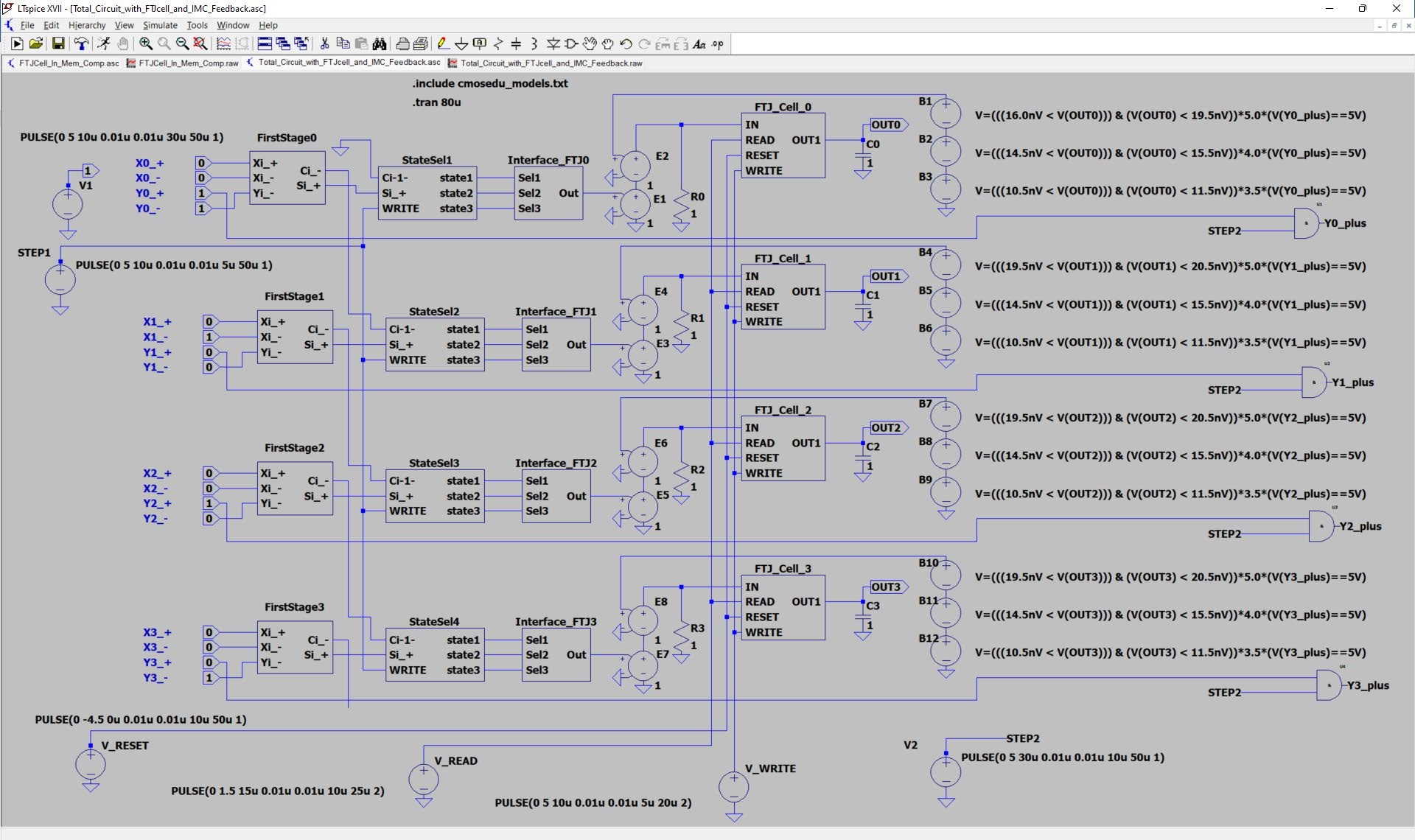
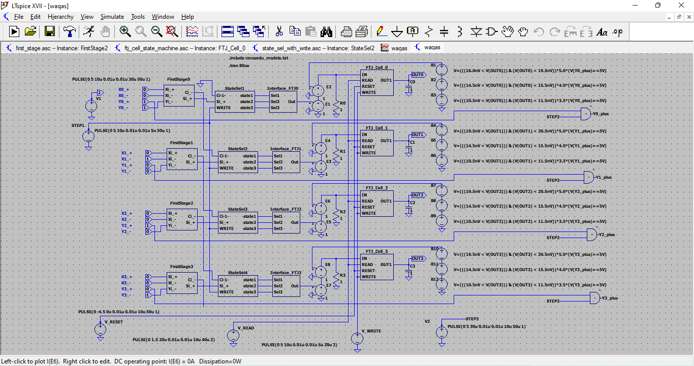
II) Complete ternary adder circuit for FTJ cells comprising step 1 and step2
The following schematic in figure 12 shows the complete circuit for the addition of the ternary numbers in which the circuit for the calculation of the first step was extended on the right side about the circuit for an in-memory-computation in such a sense that the current sate of each FTJ_cell is read out after the reuslt of the first step was concluded. Depending on the measured state each cell is switched to the neighbouring higher state if the the ternary input digit Yi_+ is equal to 1.
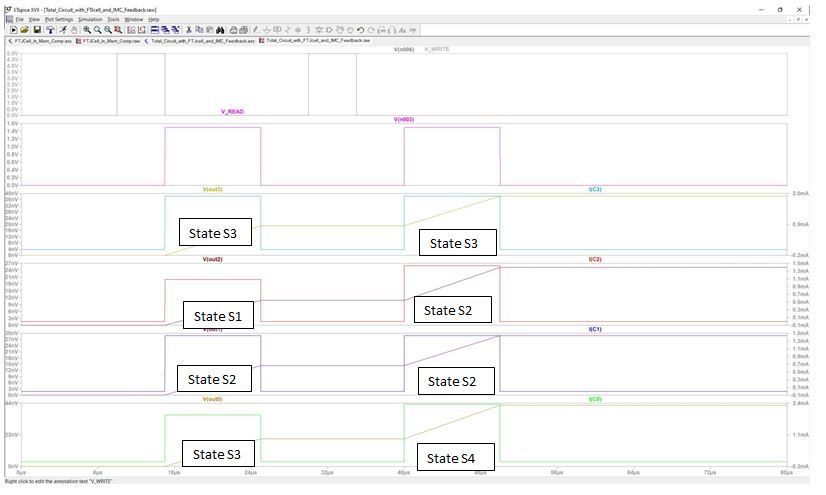
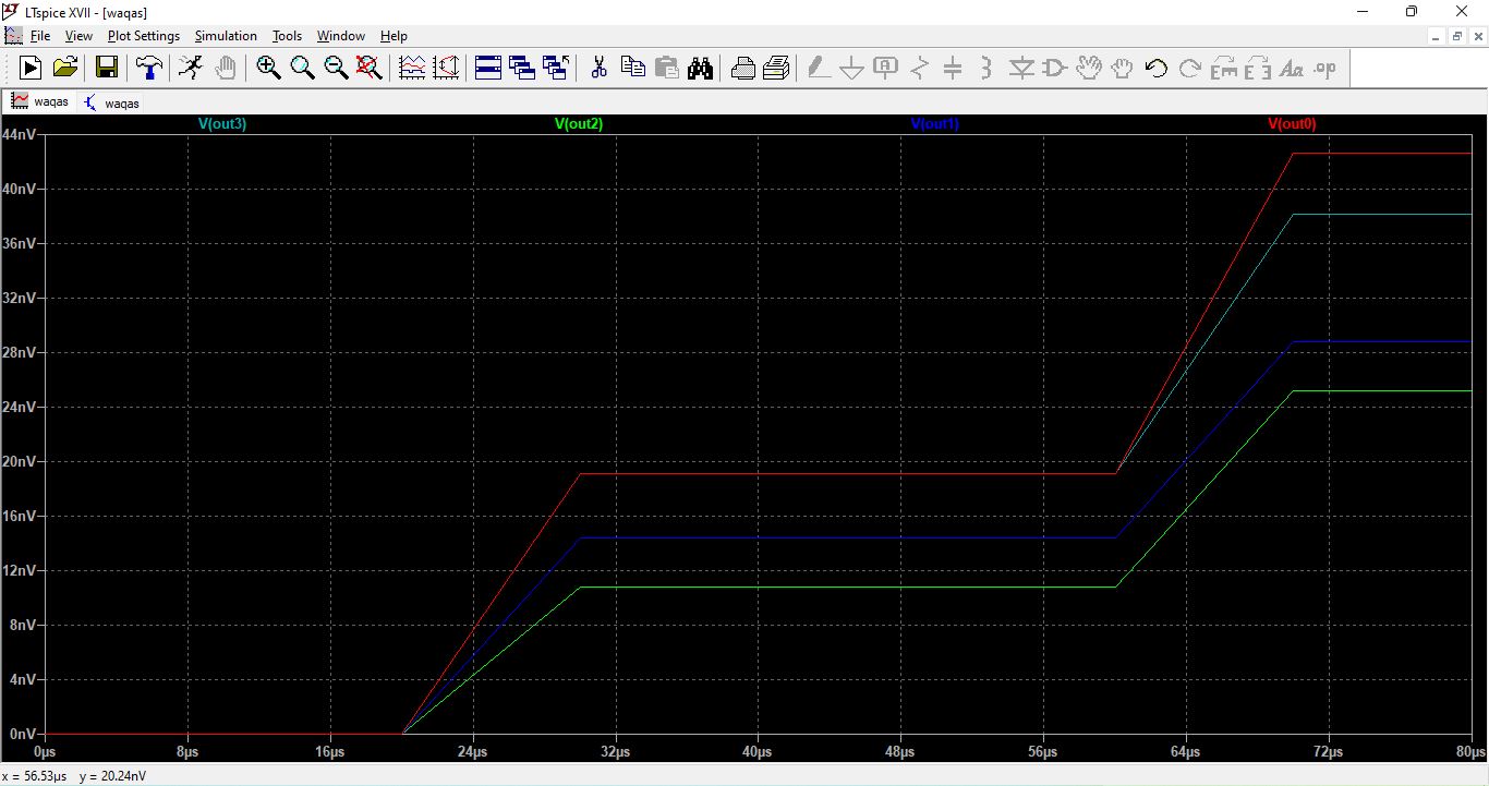
The result of the simulation of this circuit is shown in the next figure 13. At the beginning the FTJ cells are written with the result of the first step. As result the written states are read out with the first active pahse of V_READ. V(out3) and I(C3) are shown at the same pane for digit position 3, in the other three panes below the result for the other digit positions are shown. After the second write/read sequence starting at 30 µs, the second step and the feedback path of the in-memory compute operation is carried out. We can detect that only for digit position 0 and 2 we have a state transfer from S3 to S4, resp., from S1 to S2. In the other digit positions the states are kept. This corrresponds to the addition of Y+ = 0101.
Results and Analysis
Simulation results show that the CMOS full adder consistently outperforms the XOR-XOR based adder. Key observations include:
- Propagation Delay: CMOS architecture had lower average delay per transition.
- Power Dissipation: CMOS full adder showed better energy efficiency with lower dynamic power consumption.
The XOR-XOR design, despite its compactness, exhibited higher delays and power usage. The primary cause of performance degradation is traced to the pull-down resistors, which introduce additional power paths and slow down logic transitions [9].
Nonetheless, the XOR-XOR circuit’s design reveals potential for optimization in low-area or low-cost applications where absolute performance is not the critical factor. Its transistor-efficient nature could benefit ultra-dense VLSI systems with appropriate compensations.
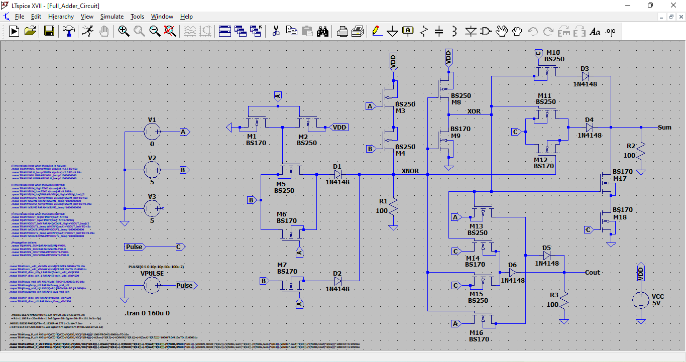
This figure shows the schematic design of the XOR-XOR based 18-transistor full adder implemented in LTSpice. The logic includes two XOR gates and carry-generation logic using MOSFETs. BS170 and BS250 models are used to simulate nMOS and pMOS behavior. Pull-down resistors are added for proper logic-level stabilization. The setup is used for transient simulation of logic inputs.
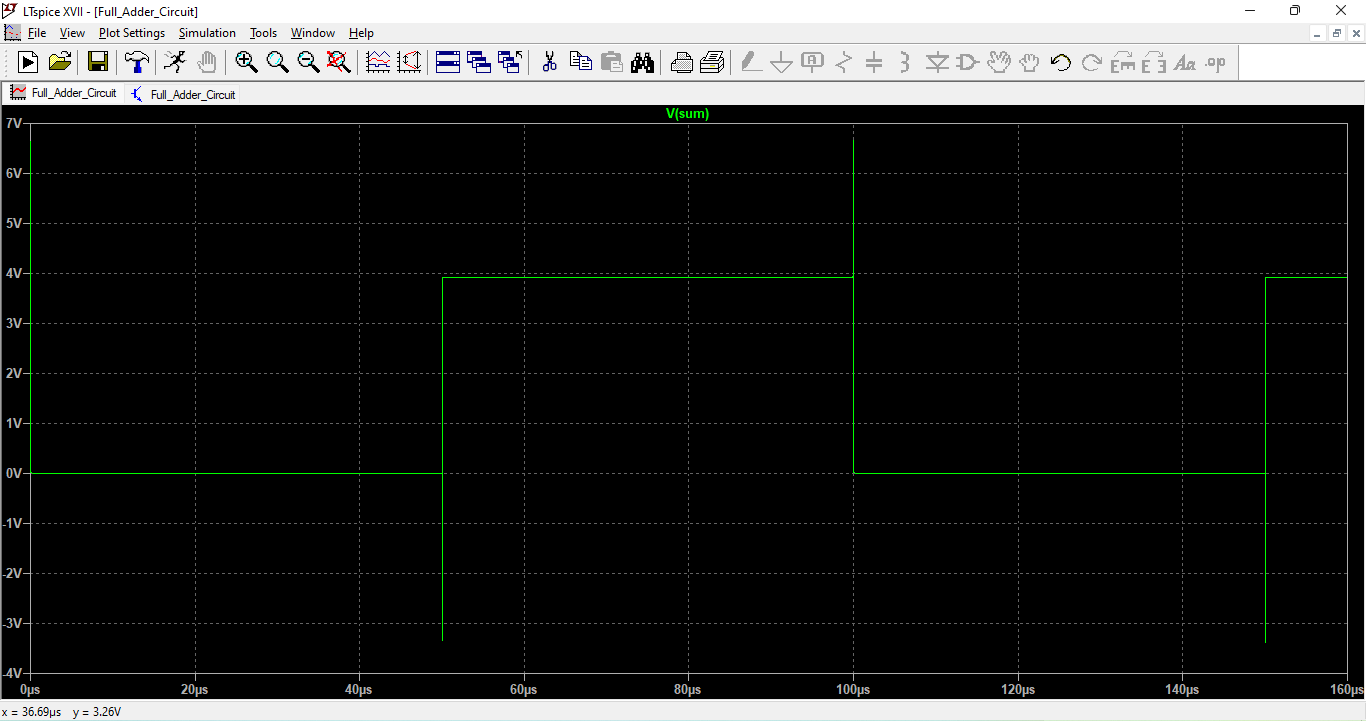
The waveform in this figure represents the SUM output of the full adder in response to all 16 input combinations. The SUM output toggles correctly based on the XOR logic behavior of inputs A, B, and Cin. Some delay is observed due to transistor switching and resistive loading. The waveform confirms logical correctness of the SUM output. Glitches, if any, are related to signal transitions.
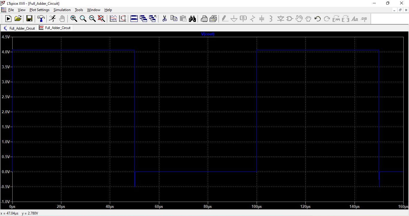
This figure displays the output waveform of the Carry signal from the full adder. The waveform transitions validate correct logical operation with respect to input combinations. Slight delays and slope variations are visible due to MOSFET charging/discharging paths. The Carry output confirms that the design correctly identifies when two or more inputs are high. Performance is consistent with expected logic truth tables.
This schematic illustrates the memory (Mem) component of the FTJCell modeled in LTSpice using the .machine command. States are defined using finite automata, and transitions are triggered by input voltages. Inputs include READ, WRITE, RESET, and IN. Each state corresponds to a different programmed logic level. The FTJ behavior is encoded using conditional state transition rules.
You can download the Project files here: Download files now. (You must be logged in).
The waveform shows output voltage responses of the FTJ memory cell to the control and input signals. State changes occur based on WRITE/IN pulses with predefined conditions. Outputs demonstrate state-dependent behavior matching the automata model. Voltage levels correspond to memory states like S0, S1, S2, etc. The results verify successful simulation of memory write/read cycles.
This schematic presents the full FTJCell model integrating the Mem component and control logic. Inputs like READ, RESET, WRITE, and IN are routed to the automata block. The complete cell simulates realistic switching between states with defined voltage thresholds. It provides a programmable logic memory function. The setup helps validate LTSpice’s .machine capabilities.
This figure shows the voltage output waveforms from the complete FTJCell simulation. Output node voltages reflect the current state of the cell in response to sequential input commands. The waveform highlights transitions between states during read/write cycles. The voltage levels confirm correct execution of automata rules. The simulation proves FTJ-based memory logic operability in LTSpice.
Conclusion
This study provides a comprehensive comparison between an XOR-XOR based 18-transistor full adder and a conventional CMOS full adder design using LTSpice simulations. The XOR-XOR design, while compact, exhibits higher propagation delays and greater power dissipation compared to its CMOS counterpart. This trade-off is largely attributed to the use of pull-down resistors, which introduce additional resistance paths and reduce switching efficiency. Despite these drawbacks, the XOR-XOR structure offers a foundation for area-efficient digital logic implementations.
In addition to the full adder comparison, the project explores the modeling of Ferroelectric Tunnel Junction (FTJ) cells as finite automata within LTSpice. The use of the .machine command enables the simulation of complex state-dependent behaviors, which is particularly valuable for memory cell design. Simulations demonstrate that FTJ cells can effectively switch states under specific voltage stimuli, confirming their potential in non-volatile memory applications.
Both parts of the project—adder design and FTJ modeling—showcase the versatility of LTSpice in simulating digital and memory circuits. While the XOR-XOR adder needs further optimization, the FTJ model establishes a framework for future integration of emerging memory technologies. Overall, this research contributes to the ongoing exploration of compact digital logic and state-based memory cell architectures in VLSI systems [10].
References
- Radhakrishnan, D. (2001). “Low-voltage low-power CMOS full adder.” IEE Proceedings – Circuits, Devices and Systems.
- Zimmermann, R., & Fichtner, W. (1997). “Low-power logic styles: CMOS versus pass-transistor logic.” IEEE Journal of Solid-State Circuits.
- Chang, C. H., Gu, J., & Zhang, M. (2005). “A review of 0.18-μm full adder performances for tree structured arithmetic circuits.” IEEE Transactions on VLSI Systems.
- LTSpice XVII Documentation. Analog Devices.
- Zhuang, N., & Wu, H. (1992). “A new design of the CMOS full adder.” IEEE Journal of Solid-State Circuits.
- Islam, M. T. et al. (2018). “Design of 1-bit Full Adder Using Modified 16 Transistor Based Multiplexer Logic.” International Journal of Electronics and Electrical Engineering.
- Balasubramanian, P. et al. (2014). “A survey of low power full adder topologies.” Microelectronics Journal.
- Rabaey, J. M. (2003). Digital Integrated Circuits: A Design Perspective.
- Lee, C. H. et al. (2004). “Energy-efficient full adder cell design using pass-transistor logic.” IEICE Electronics Express.
- Weste, N. & Harris, D. (2010). CMOS VLSI Design: A Circuits and Systems Perspective.
You can download the Project files here: Download files now. (You must be logged in).


Responses