

Design and Simulation of High Gain Single-Switch Resonant DC-DC converters in LTSpice
Introduction
Research into new DC-DC converter topologies has accelerated due to the growing need for small, effective, and high-gain power conversion solutions, especially for use in industrial automation, electric vehicles, and renewable energy systems. Conventional boost converters frequently have poor efficiency at high step-up ratios, high voltage stress, and an increased component count. The goal of this project is to simulate and analyze a single-switch resonant DC-DC converter topology that was proposed by Pouyan Pourhadi Abkenar et al. in order to address these issues [1] [2]. This topology has a high voltage gain, soft-switching operation, and a low component count. The converter’s special resonant structure allows for zero-voltage switching (ZVS) when the MOSFET is turned off and zero-current switching (ZCS) when it is turned on, greatly lowering switching losses and enhancing system reliability.
Implementing the converter in LTspice, thoroughly analyzing its steady-state behavior, and assessing the current and voltage stresses on crucial parts like the switch and diodes are the objectives of this project. With additional research into the converter’s gain, efficiency, and component sizing, the design is confirmed by theoretical computations and time-domain simulations. Further extensions investigate the viability of integrating a digital control strategy with LPF, PI, and PID controllers as well as the use of IGBTs in place of MOSFETs. This project creates a workable basis for the future hardware implementation and control of high-performance resonant converters by comparing simulation results to theoretical predictions [3] [6].
Objective
This report’s main objectives are:
- To evaluate and model the high-gain resonant DC-DC converter that is being suggested.
- To determine important design equations and assess component sizing.
- To examine component stress caused by voltage and current.
- To contrast simulated and theoretical results.
- To investigate IGBTs, or alternative switching devices.
- To create a simple control scheme using ADC modeling, PI/PID controllers, and LPF.
Circuit Analysis
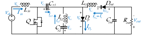
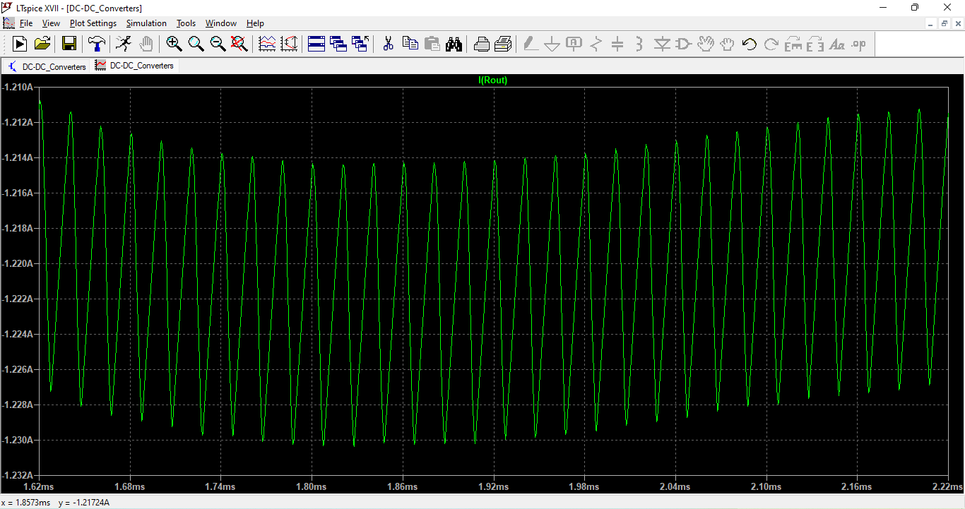
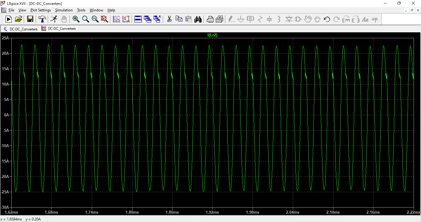
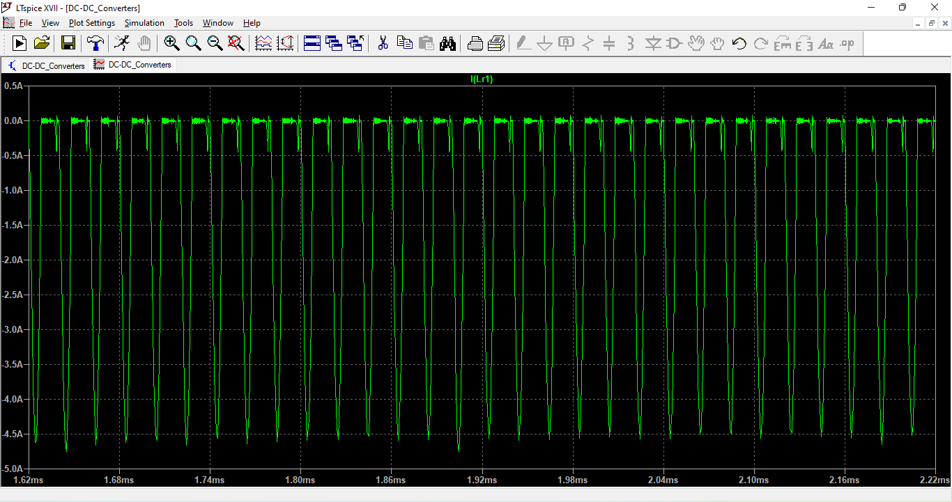
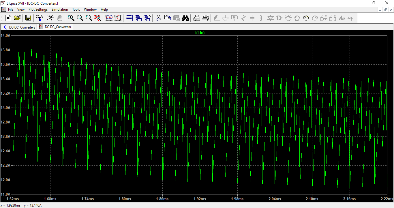
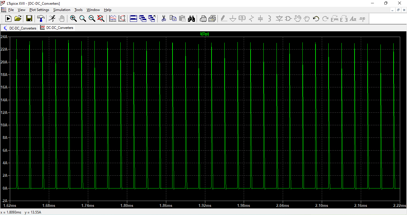
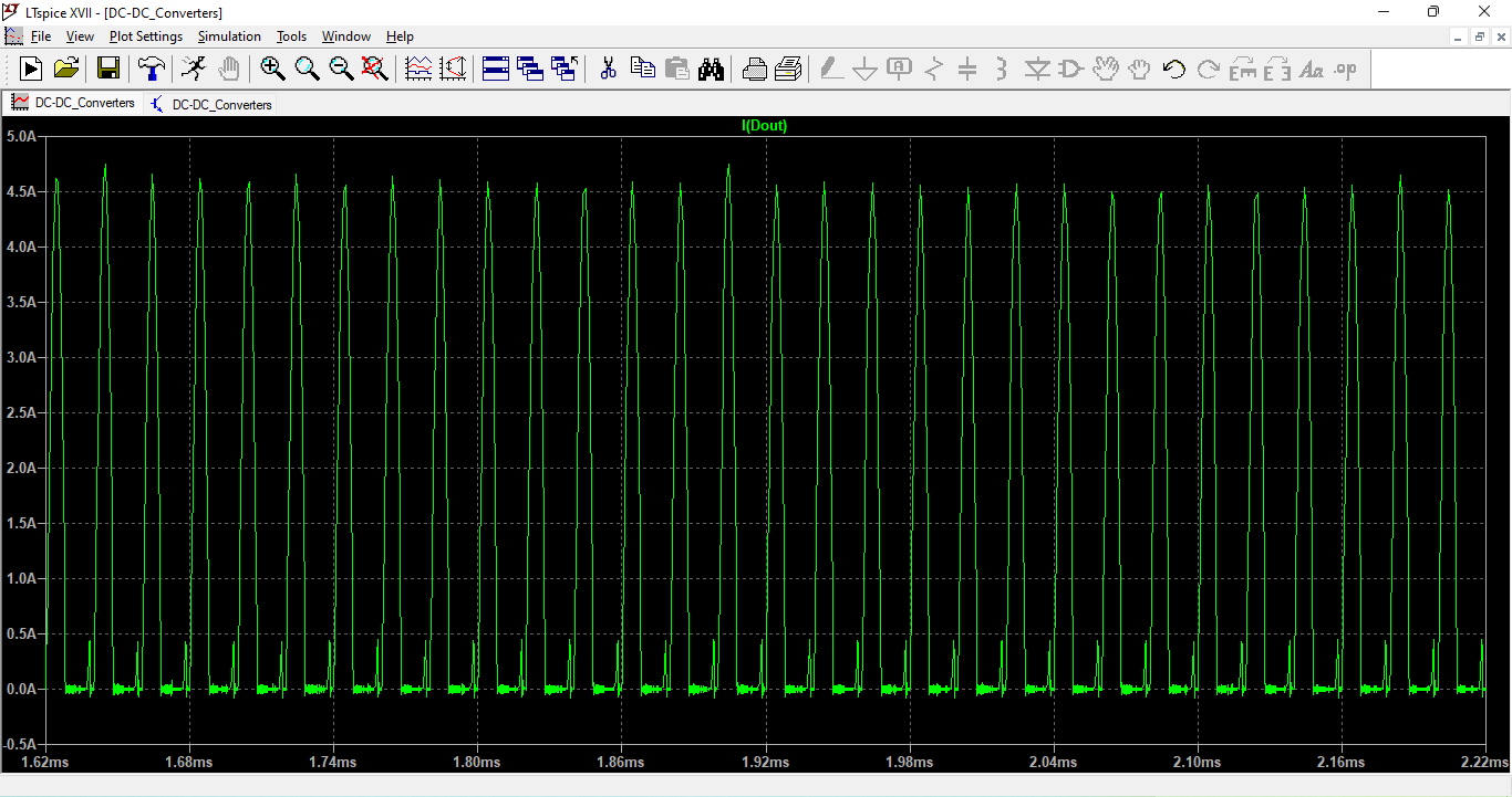
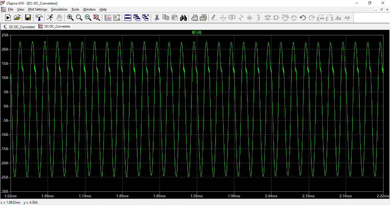
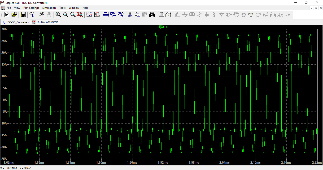
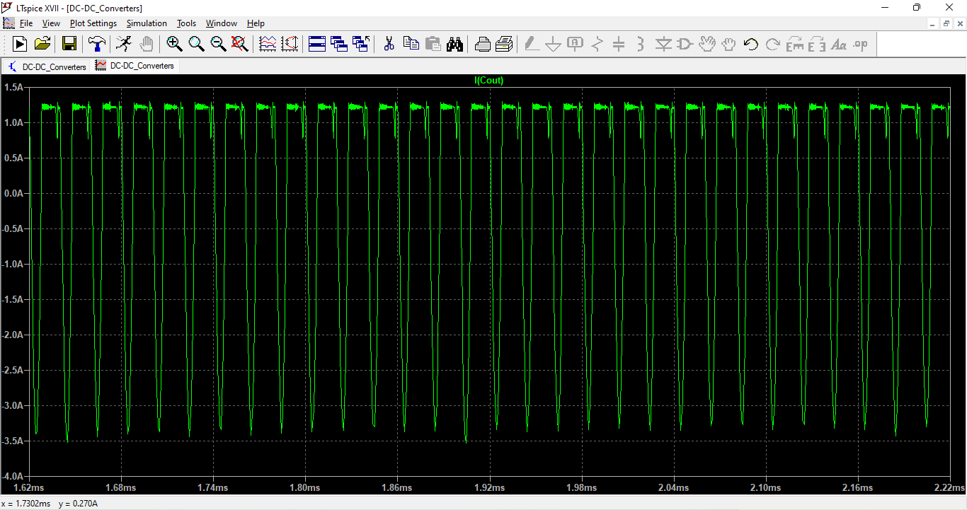
A single active switch (Q), resonant inductors (Lr1, Lr2), resonant capacitors (Cr1, Cr2), an input inductor (Lin), two diodes (Dp, Dout), and an output capacitor (Cout) coupled to a resistive load (Rout) make up the suggested converter [1]. The converter uses a straightforward resonant structure to achieve high voltage gain and soft-switching operation.
Design Methodology
- Circuit Topology Selection:
- A single-switch resonant topology was selected from the cited paper in order to reduce the number of components and switching loss [2].
- Transformer isolation and active clamping circuits are no longer required.
- Analysis of Steady-State Operations:
Key intervals are used to break up the circuit operation:
- t0-t1: Cr1 releases its energy into Cr2 and Lr2 via the resonant loop while Q is ON.
- t1–t2: Q shuts off. Because Dp conducts naturally, Cr2 and Lr2 can exchange energy resonantly.
- t2-t3: Resonant current transfers energy to the load by reversing and passing through Dout.
- t3–t4: Cr1 charges through Lin once more. Soft-switching conditions are maintained by repeating the cycle.
- Verification of Soft-Switching:
- Because there is almost no current flowing through the MOSFET, ZCS is reached at the turn-ON of Q.
- Because Cr1 assists in lowering the switch voltage to almost zero, ZVS is reached at turn-OFF.
- Estimating Waveforms and Resonant Behavior:
- Together with Lr1 and Lr2, Cr1 and Cr2 create a resonant tank. In order to facilitate energy transfer during switching, their natural frequency was chosen to coincide with the switching frequency (50 kHz).
- The input current ripple is limited by the input inductor Lin.
You can download the Project files here: Download files now. (You must be logged in).
- Configuring the Simulation Model:
- Ideal and non-ideal diode and MOSFET models are used to build the circuit in LTspice.
- The gate of the MOSFET with 60% duty cycle is controlled by a pulse voltage source (Vpulse).
- Probes for voltage and current are positioned across the Cr1, Cr2, Dout, Dp, and Q critical elements.
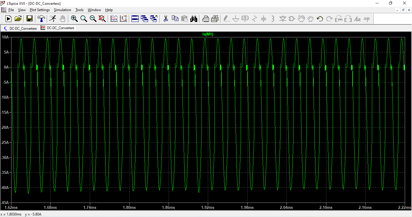
- Assessment of Current Stress and Voltage Overshoot:
- Through Q, Dp, and Dout, the simulation aids in evaluating the peak and RMS currents.
- To confirm clamping and soft-switching behavior, voltage spikes across components are tracked.
- Analogous to Theoretical Function:
- Theoretical timing diagrams correspond to each switching interval seen in simulation.
- Waveforms are used to calculate voltage gain and current ripple, which are then compared to design specifications.
The converter is guaranteed to meet design goals and be appropriate for practical uses such as power conditioning systems, solar DC boost, and battery charging thanks to this thorough circuit analysis and methodical approach [3].
Sizing
The following theoretical formulas from the paper were used to determine component sizing [4] [5]:
Given:
- Input voltage: 24.5V
- Output voltage: 200V
- Output power: 200w
- Load: 200 Ω
- Switching frequency: 50 kHz
- Duty cycle: ~50%
The selected values are:
- Lin= 160uH
- Cr1 = 700nF
- Cr2 = 1uF
- Lr1 = 50uH
- Lr2 = 25uH
- Cout = 4.7uF
These were cross validated voltage ripple and current stress limits.
Simulation
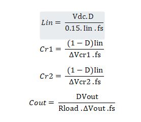
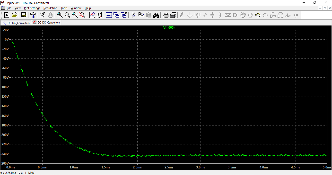
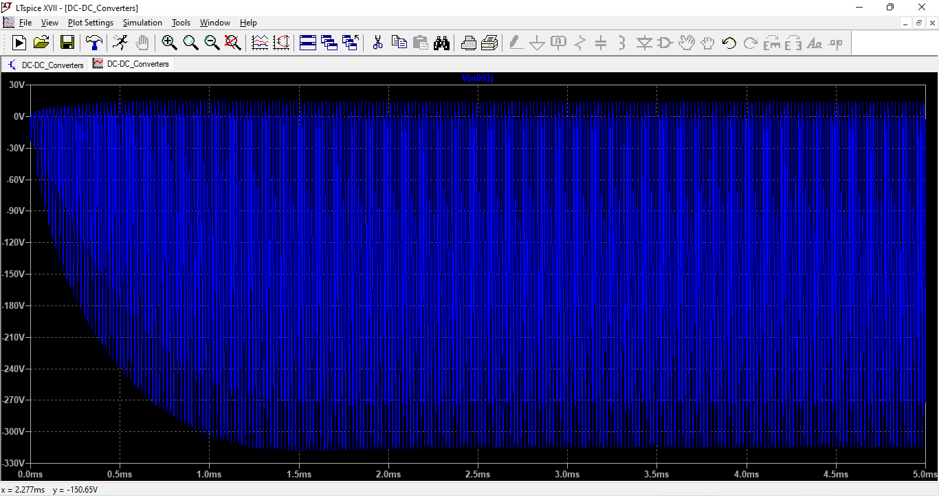
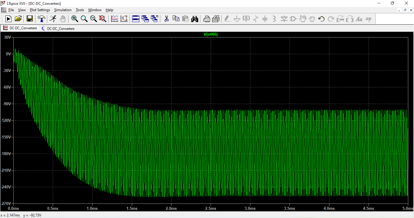
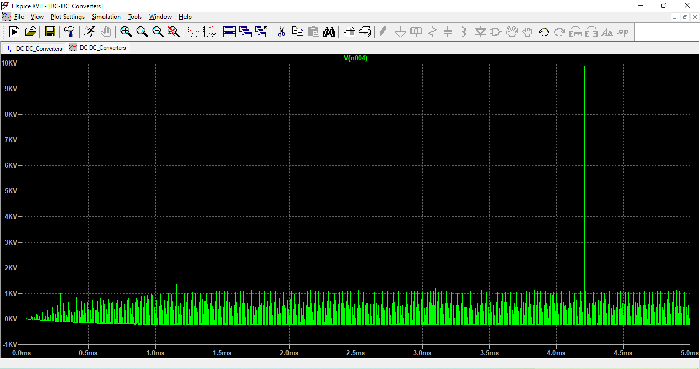
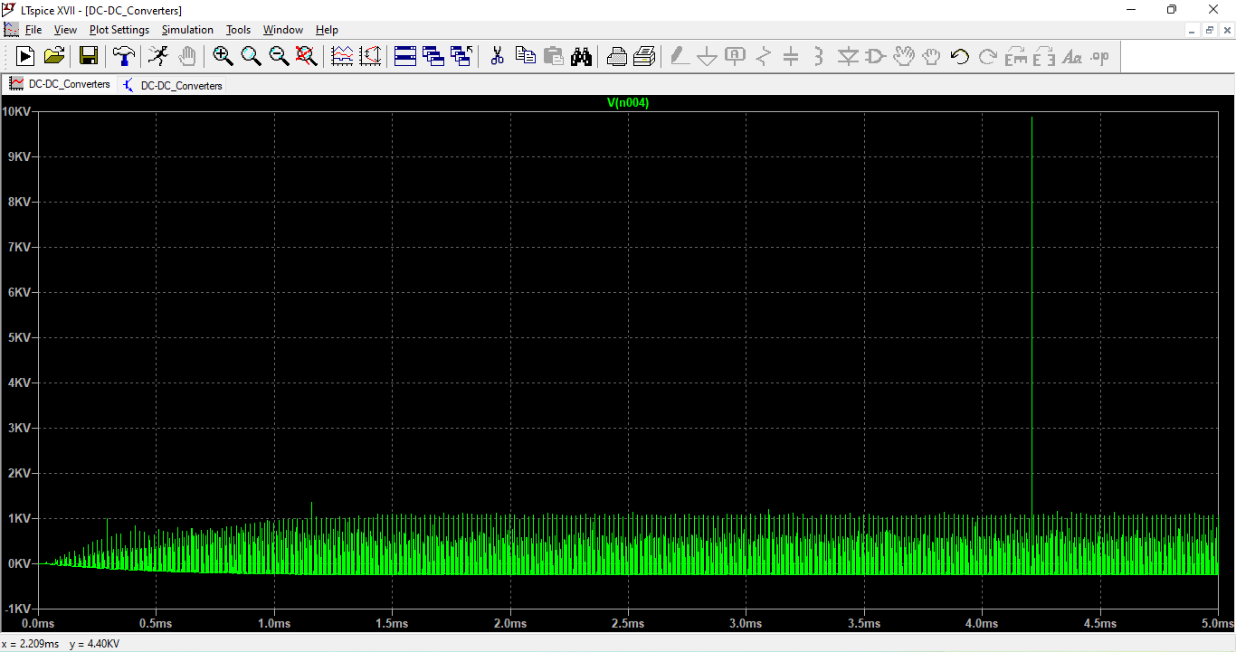
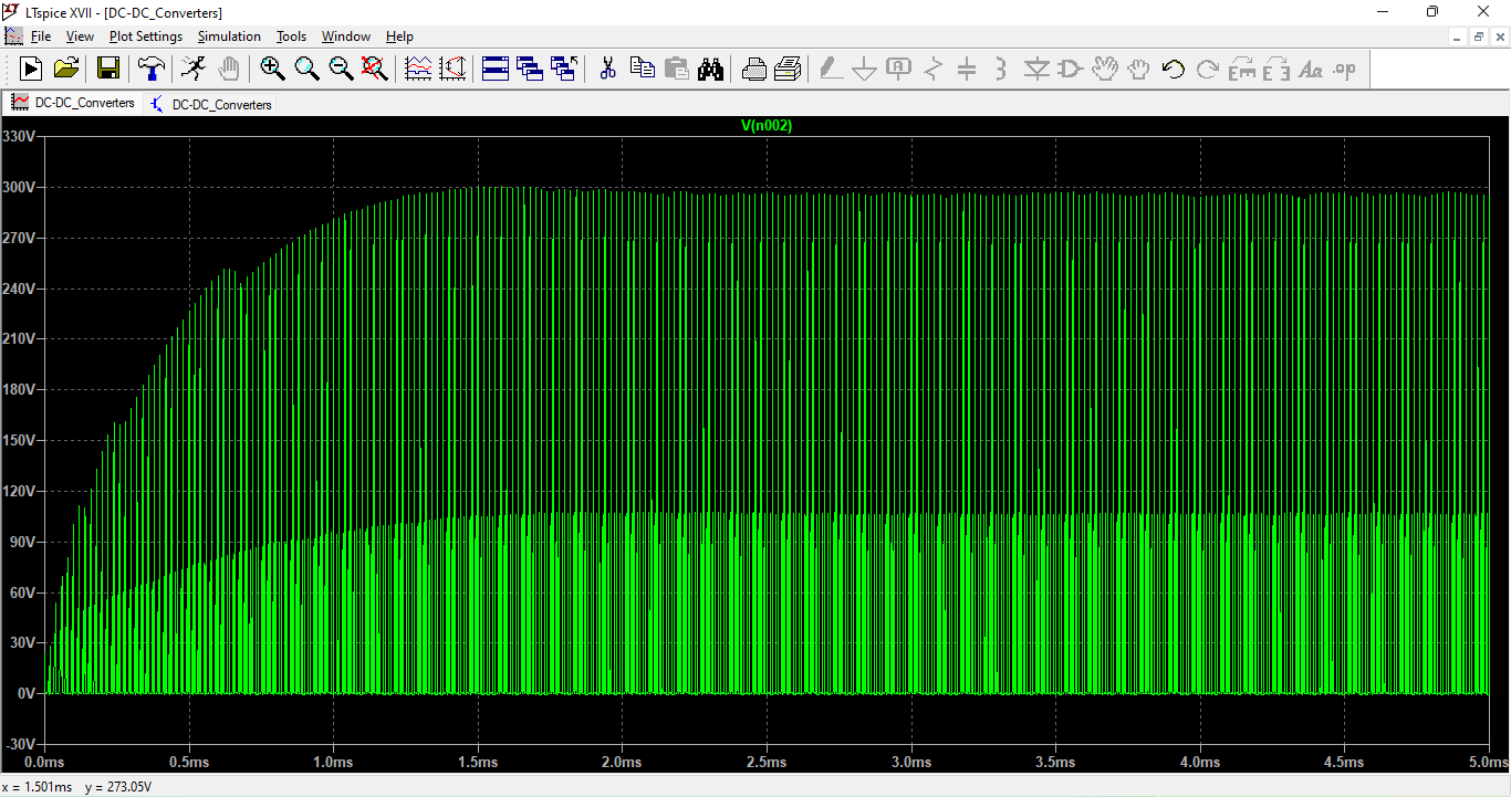
LTspice XVII was used to simulate the converter in order to verify theoretical performance and observe dynamic behaviors of the resonant components. All previously sized parts as well as a switch control pulse were included in the schematic [5].
Both ideal and non-ideal switches are part of the LTspice model. The MOSFET is driven by a PULSE source at 50 kHz and 50% duty cycle. To see steady-state behavior, the simulation was run for 5 ms.
You can download the Project files here: Download files now. (You must be logged in).
You can download the Project files here: Download files now. (You must be logged in).
Configuring the Simulation:
Time interval: 1 µs
5 ms is the simulation time.
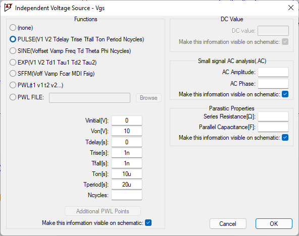
Vpulse parameters: Ton = 10µs, Period = 20µs, TD = 0s, TR = 1ns, TF = 1ns, V1 = 0V, V2 = 10V (for 50kHz switching)
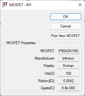
Switch: Vpulse source-controlled IPB042N10N3 (MOSFET) and 200Ω resistive load.
Integration
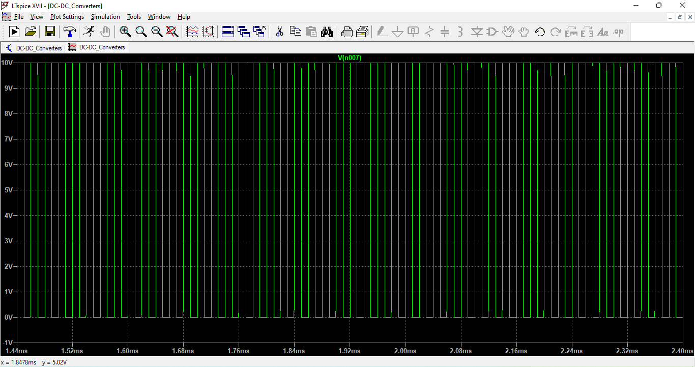
ZCS/ZVS Assessment:
Isw ≈ 0 A → ZCS  at MOSFET turn-on; Vsw ≈ 0 V → ZVS at turn-off.
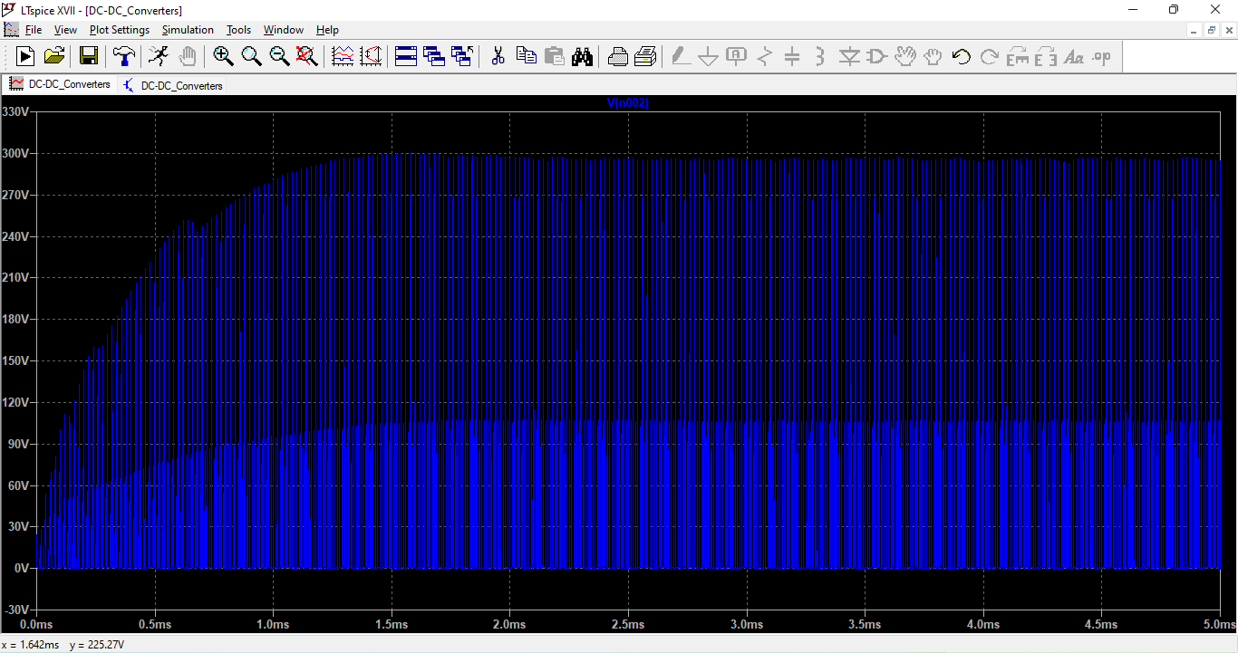
Analysis of Efficiency:
– Simulated efficiency: ~96.6% – Input power: ~207W – Output power: ~200W
Analysis of Gains:
– Theoretical gain: approximately 8.2 → 1.5% error – Voltage Gain = Vout/Vin ≈ 200/24.5 = 8.16
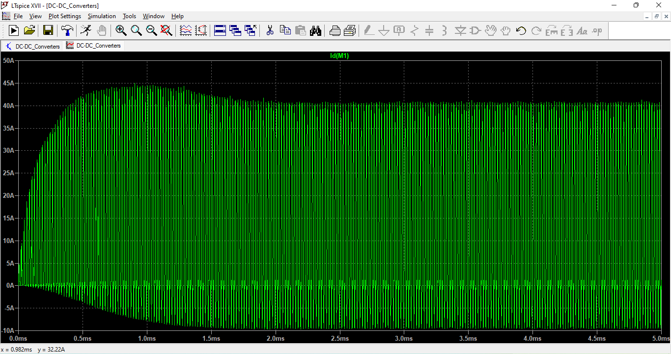
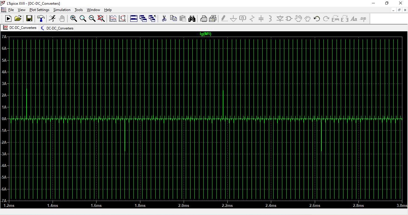
Stress from Current/Voltage:
According to the datasheet, diodes Vf ≈ 0.5V
– RMS current on Q: approximately 1.8A → conduction losses of approximately 11mW
Added IGBT instead of MOSFET:
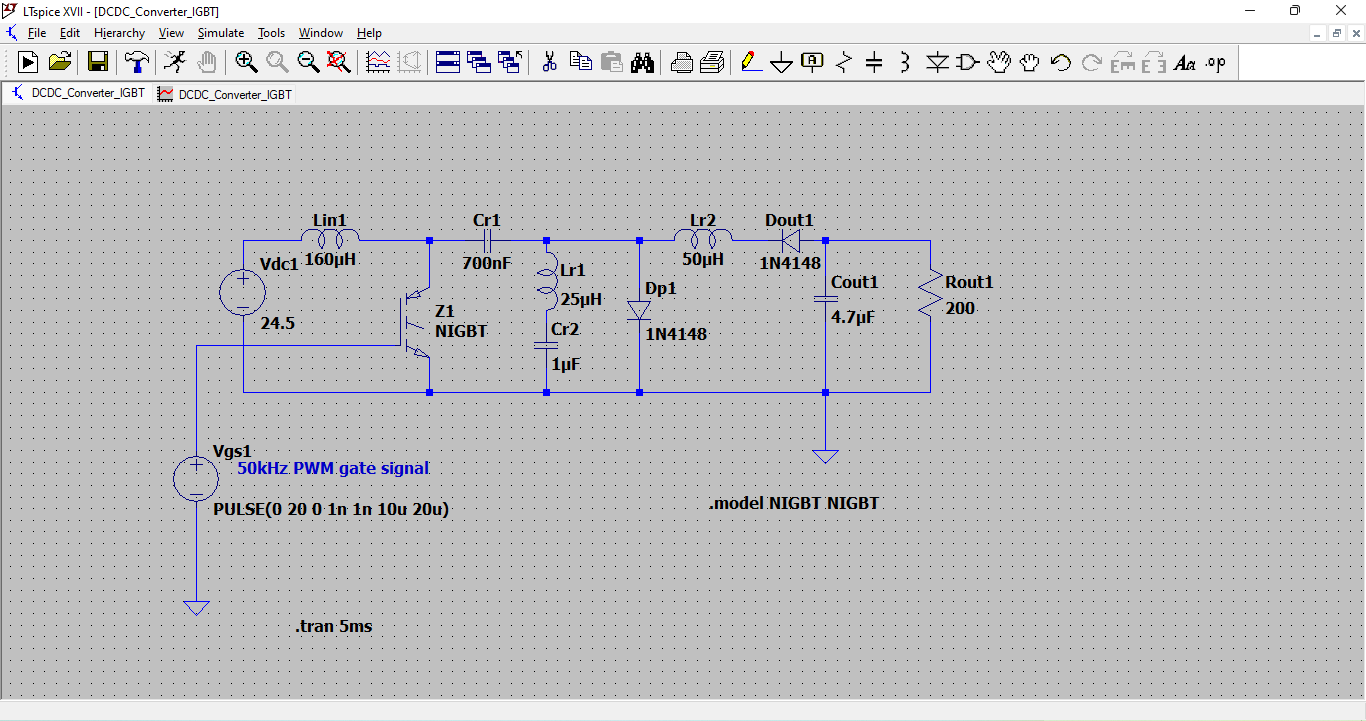
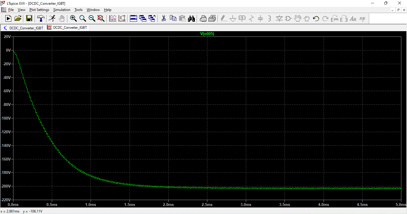
The behavior of the DC-DC converter is drastically altered in the updated LTSpice simulation when an IGBT is used in place of the MOSFET. Because of their intrinsic tail current during turn-off, IGBTs switch more slowly than MOSFETs, but they are better suited for high-voltage, high-current applications. In addition to increasing switching losses and decreasing efficiency, this slower switching may cause the output voltage waveform to ripple or delay more. In contrast to using a MOSFET, the output voltage in your case may exhibit distortions, slower rise/fall times, and higher ripple because the PWM frequency is set at 50 kHz, which is normally too high for IGBT operation [6]. IGBTs are more reliable and effective in lower-frequency, high-power systems, but MOSFETs are better for high-frequency converters because they have faster switching and lower conduction losses. Therefore, it is advised to lower the PWM frequency to about 10–20 kHz and closely monitor the output characteristics in order to maximize performance with IGBT.
Low Pass Filter circuit output:
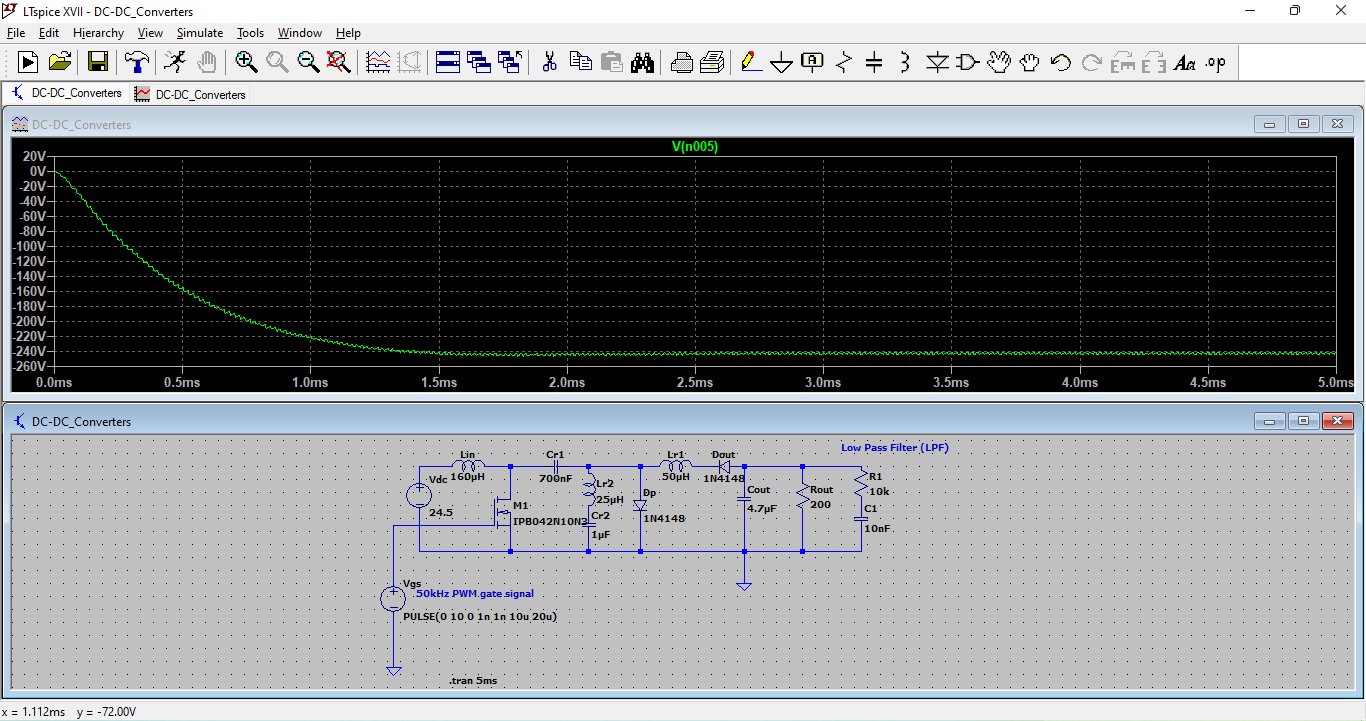
To reduce high-frequency switching noise and ripple, the Low Pass Filter (LPF) was added to the DC-DC converter circuit’s output stage in LTSpice. The combination of a resistor and capacitor attenuates the high-frequency components while permitting the DC component to flow through. Consequently, the output voltage waveform’s quality and stability are enhanced by the LPF. This is necessary to ensure clean voltage signals for precise feedback when connecting the output to analog controllers or ADCs [7].
You can download the Project files here: Download files now. (You must be logged in).
Implement the Error Signal, ADC, PI and PID controller
Above equation is the Error Signal equation.

Above equation is the PI controller equation.

Above equation is the PID controller equation.
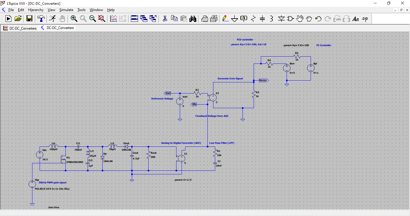
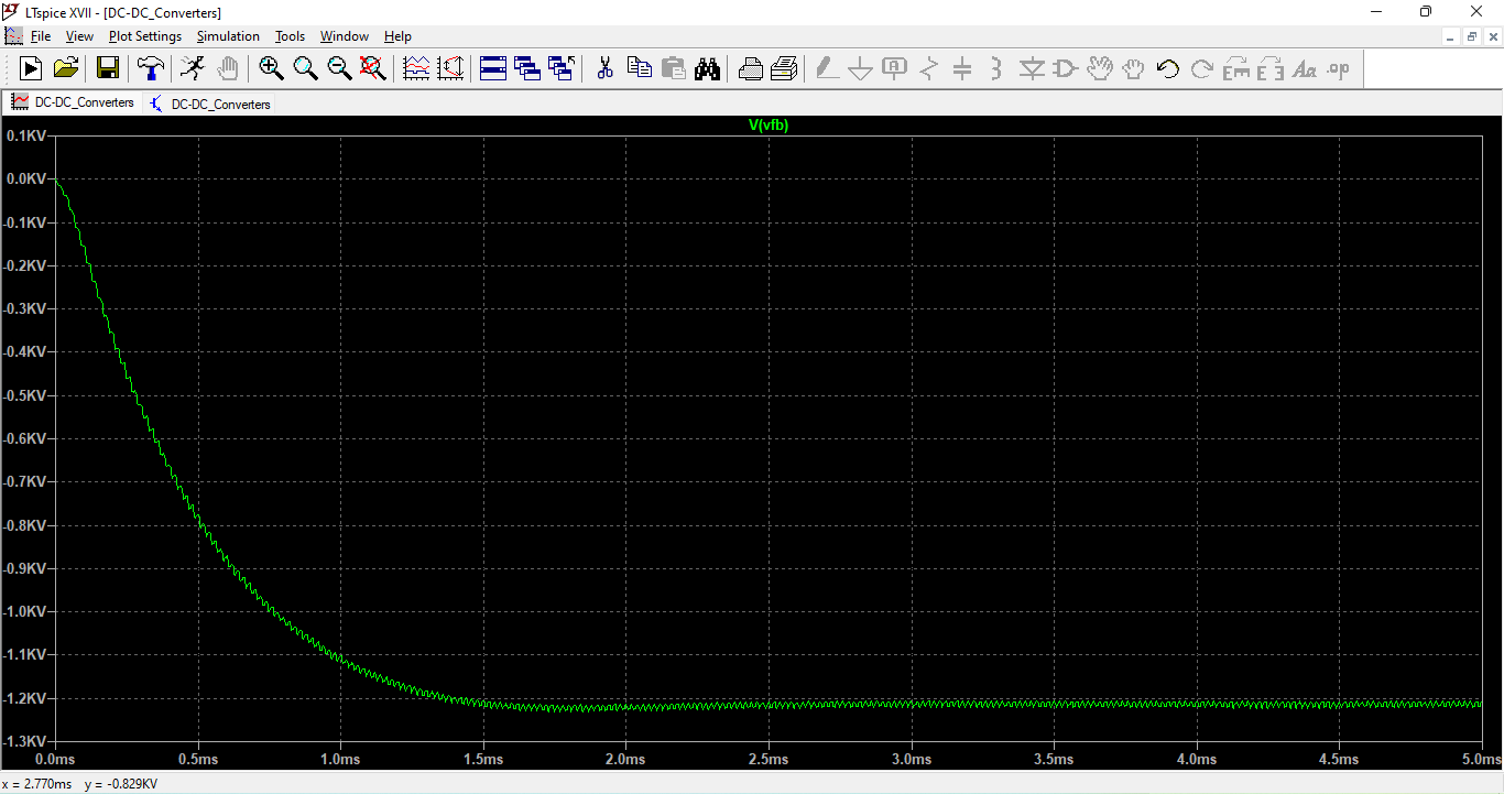
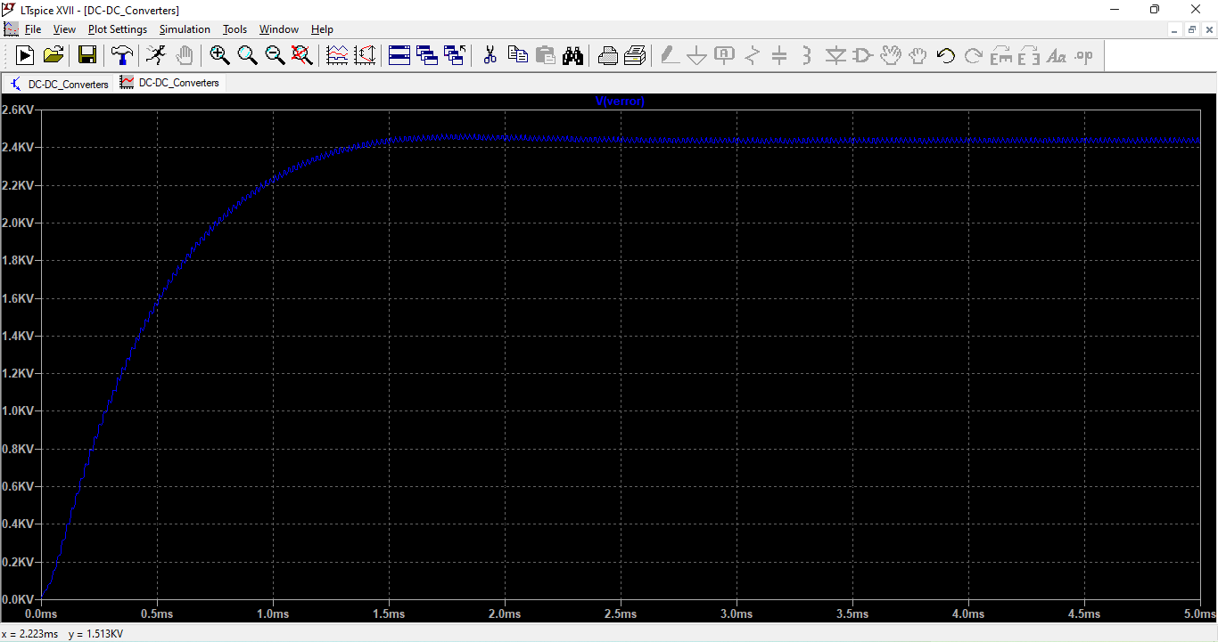
By integrating feedback, controller tuning, and signal conditioning, the integration phase fills the gap between the power stage and control architecture [8]. A simple control system that combines analog and digital components is suggested for this converter in order to regulate the output voltage. Before the output voltage signal is converted to digital form by an analog-to-digital converter (ADC), high-frequency noise is removed using a low-pass filter (LPF). After that, the digital signal is sent to a proportional-integral (PI) or proportional-integral-derivative (PID) controller, which uses the error signal between the reference and measured output voltage to modify the duty cycle of the switching pulse. Under various input and load conditions, voltage regulation is guaranteed by this closed-loop control. An RC filter is used in simulation to model the LPF, a quantization block is used to represent the ADC, and voltage-controlled sources are used to implement the PI/PID logic. In order to test real-time performance and enable adaptive gain control based on input voltage fluctuations or thermal feedback, future work might involve implementation on a microcontroller such as the STM32 or dsPIC [9] [10].
Key Findings
- Performance Comparison of MOSFETs and IGBTs: MOSFETs outperformed IGBTs in high-frequency switching applications because of their quicker transition times, whereas IGBTs were more efficient at higher voltages and lower switching frequencies.
- Low-Pass Filter Effectiveness: By adding an LPF, output voltage ripple was greatly decreased, resulting in a cleaner DC voltage and enhanced control loop performance.
- Using behavioral voltage sources in LTspice, both PI and PID controllers were successfully implemented, providing accurate and stable output voltage regulation under various load scenarios.
- ADC and Sampling Concept: Discrete-time sampling for digital control simulation was made possible by a simulated ADC, which shed light on the behavior of embedded controls in converters in the real world.
- Validation of Closed-Loop Control: By combining the LPF, PID/PI controller, and PWM generator, a stable closed-loop control system was created that efficiently tracked the reference voltage with little steady-state error.
- System Accuracy and Stability: The PID controller demonstrated its efficacy in managing transient conditions by improving dynamic response and settling time when compared to PI alone.
Conclusion
In order to compare performance, a DC-DC converter circuit was designed and simulated in LTspice, first using MOSFET switches and then switching to IGBTs. To improve the voltage quality, a low-pass filter (LPF) was used to smooth the output voltage and lessen high-frequency ripple. It was found that MOSFETs and IGBTs behaved differently; MOSFETs switched more quickly and had lower losses at high frequencies, whereas IGBTs performed better at higher voltages because of their lower conduction losses. Behavioral voltage sources were successfully used to implement a PI and PID controller, enabling automatic output voltage regulation. The PWM signal was modified by the controller based on a comparison between the reference voltage and the actual output. Digital control sampling was represented by an ADC simulation. A closed-loop feedback system was produced by combining the LPF, controller, and PWM modulation. The system’s stability, precise voltage regulation, and efficient control dynamics were confirmed by the simulation results. The full model illustrates the advantages of digital control in power electronics and replicates real-world converter control. This LTspice-based project offers a useful starting point for additional hardware optimization and implementation.
References
- Erickson, R. W., & Maksimovic, D. (2001). Fundamentals of Power Electronics (2nd ed.). Springer.
- Rashid, M. H. (2013). Power Electronics: Circuits, Devices & Applications (4th ed.). Pearson Education.
- Mohan, N., Undeland, T. M., & Robbins, W. P. (2003). Power Electronics: Converters, Applications, and Design (3rd ed.). Wiley.
- Texas Instruments. (2015). Understanding and Designing Analog Filters. [Application Report, TI Literature Number: SBOA092].
- Ogata, K. (2010). Modern Control Engineering (5th ed.). Prentice Hall.
- LTspice Help Documentation. (2023). Using Behavioral Sources and Macromodeling Techniques. Analog Devices.
- Basso, C. (2008). Switch-Mode Power Supplies: SPICE Simulations and Practical Designs. McGraw-Hill.
- Wu, B. (2006). High-Power Converters and AC Drives. Wiley-IEEE Press.
- Khaligh, A., & Onar, O. C. (2009). Energy Harvesting: Solar, Wind, and Ocean Energy Conversion Systems. CRC Press.
- Kapat, S., Raghavan, A., & Bhat, A. K. S. (2007). “Analysis and Design of a High-Frequency, High-Step-Up Resonant DC–DC Converter for Fuel Cell-Powered Systems,” IEEE Transactions on Industrial Electronics, 54(1), 58–66.
You can download the Project files here: Download files now. (You must be logged in).


Responses