

PCB Design and Development of RF Power Detector Circuit
Author: Waqas Javaid
Abstract
This report presents the complete design, schematic development, and PCB implementation of an RF power detector circuit using Altium Designer. The objective of this project was to design a robust, reliable, and efficient circuit capable of detecting RF power levels and providing a corresponding DC output voltage. The report details the schematic development, component selection, PCB layout considerations, and implementation methodology. The design emphasizes impedance matching, noise reduction, and stable power supply distribution, ensuring accurate performance across RF frequency ranges.
Introduction
RF (Radio Frequency) power detectors are critical components in RF systems, enabling measurement, monitoring, and control of transmitted and received power levels. Applications range from communication systems, radar, RF instrumentation, and signal testing. This project focuses on developing a PCB that integrates an RF input section, filtering network, power detection IC, and DC output stage. The PCB was designed using Altium Designer, starting from schematic entry to final PCB layout and routing. The design adheres to standard RF design practices, such as controlled impedance routing, ground plane isolation, decoupling strategies, and minimizing parasitic capacitance/inductance.
Printed Circuit Boards (PCBs) are the foundation of nearly all modern electronic systems, serving as the structural and electrical platform that interconnects active and passive components. In high-frequency and RF applications, PCB design is not just about connectivity but also about maintaining signal integrity, impedance control, and minimizing noise coupling. Unlike low-frequency designs where trace routing is less critical, RF circuits demand precise placement, routing, and grounding strategies to avoid parasitic capacitances, inductive loops, and electromagnetic interference (EMI). The miniaturization of electronics has further increased the importance of optimized PCB design methodologies, as compact layouts must still achieve high performance without compromising reliability. In this context, designing a custom RF detector PCB provides an excellent opportunity to demonstrate the application of advanced design principles in schematic capture, component placement, PCB routing, power distribution, and testing strategies.

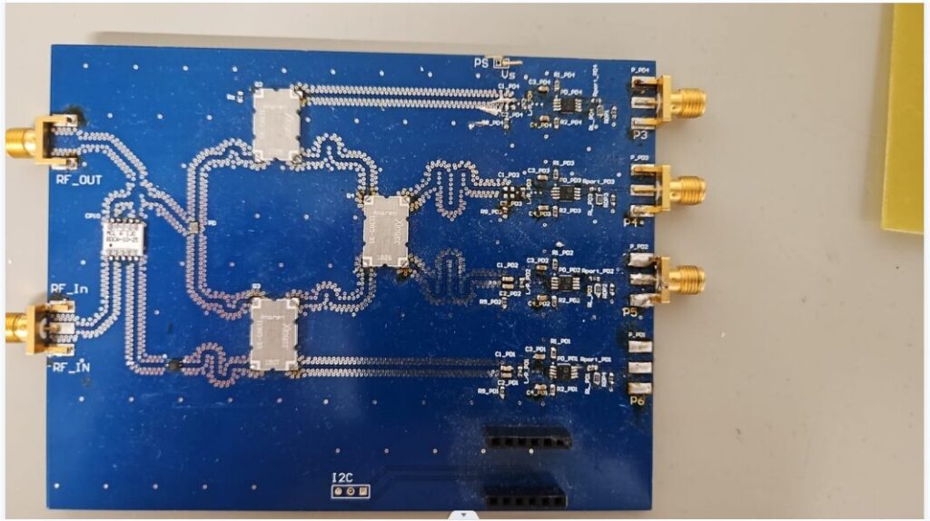
The project presented in this report focuses on the design and development of a Radio Frequency (RF) power detector circuit, implemented using Altium Designer. The primary objective of the circuit is to detect incoming RF signals and convert them into a proportional DC output voltage, which can be used for monitoring and control in RF systems [1]. The developed PCB integrates a detector IC at its core, supported by a set of coupling capacitors, biasing resistors, load resistors, and decoupling networks to ensure accurate detection performance across the specified frequency range. An SMA connector serves as the input interface, allowing direct connection to RF generators or antennas, while the output node provides an easily measurable voltage. By adopting a modular and compact design, the PCB can be deployed in a wide range of RF test setups, including communication systems, instrumentation, and wireless energy transfer applications [2].

The development of this PCB required addressing several key challenges specific to RF circuit design. One major consideration was ensuring controlled impedance on RF signal traces, particularly from the SMA connector to the detector IC input pins. Incorrect impedance matching can lead to reflections, insertion losses, and distortion of the input signal, thereby reducing detection accuracy. Another critical factor was noise suppression in the power supply path, as RF detectors are sensitive to high-frequency noise and fluctuations. Decoupling capacitors had to be carefully positioned near the IC to minimize parasitic inductance and ensure stable supply voltage. Moreover, the choice of resistors and capacitors was not arbitrary; their values had to align with the IC’s recommended application circuit to ensure linearity across the expected input power range. PCB grounding strategies, such as the implementation of a continuous ground plane and minimizing via transitions in RF paths, were also crucial to achieving optimal performance. These considerations highlight the fact that RF PCB design is both a science and an art, requiring theoretical knowledge as well as practical design experience [5].
Altium Designer played a pivotal role in the execution of this project, offering a comprehensive environment for schematic capture, PCB layout, rule checking, and simulation. The tool’s ability to manage design constraints such as controlled impedance traces, clearance rules, and net class assignments ensured that the layout adhered to high-frequency standards. Electrical Rule Checks (ERC) and Design Rule Checks (DRC) were extensively used to prevent design errors such as floating nets, power-ground conflicts, or improper clearances. The 3D PCB visualization feature of Altium further aided in verifying mechanical constraints and connector alignments, ensuring that the SMA interface and IC package footprints were correctly integrated. By leveraging these advanced capabilities, the project achieved a high degree of design accuracy, manufacturability, and test readiness, minimizing risks associated with fabrication and assembly. This integration of simulation, validation, and visualization streamlined the entire workflow, making Altium Designer an indispensable tool in the methodology [3].
This report provides a comprehensive account of the design, development, and validation of the RF detector PCB. It begins with a discussion of the underlying principles of RF detection and the role of each circuit component in achieving the desired functionality. The methodology section elaborates on schematic capture, component selection, PCB routing, grounding strategies, and power distribution, followed by verification techniques applied within Altium Designer. Simulation results, fabrication considerations, and practical testing strategies are also presented to provide a holistic view of the design lifecycle. By the end of this report, readers will gain a complete understanding of the steps involved in creating a high-performance RF circuit PCB, from concept to prototype validation. Furthermore, the documentation serves as a valuable reference for engineers and students working on similar projects, highlighting both best practices and potential challenges in RF PCB design.
Objectives
To design a functional RF power detector circuit with accurate DC output corresponding to RF input power.
- To select suitable passive and active components for reliable RF operation.
- To develop a PCB in Altium Designer ensuring proper signal integrity.
- To test and validate the PCB design using RF input and DC output measurement.
Design Methodology
The methodology for developing the RF power detector circuit began with a systematic schematic capture process in Altium Designer, ensuring that each component was carefully chosen and connected according to the datasheet specifications of the RF detector IC. The schematic design included an SMA connector at the RF input to interface with test equipment or an RF signal generator. Capacitors C1 and C2 were selected as coupling capacitors to block any DC offset while allowing high-frequency AC signals to pass through without significant attenuation. Careful consideration was given to the values of these capacitors, as they directly influence the cutoff frequency and the linearity of the detector response. The IC pins were mapped one-to-one with the schematic symbols, reducing the possibility of pin mismatch errors during PCB footprint generation. Furthermore, resistors R1, R2, and R9 were integrated to limit current surges, stabilize the circuit, and configure biasing conditions. At this stage, extensive cross-verification was carried out against the IC datasheet and manufacturer’s application circuits to ensure proper design logic. The schematic was then validated using ERC (Electrical Rule Check) in Altium, confirming there were no floating nets, unconnected pins, or power-ground conflicts before moving toward PCB layout implementation.


You can download the Project files here: Download files now. (You must be logged in).
The second phase of methodology focused on component selection and strategic placement within the PCB layout. Since RF circuits are highly sensitive to parasitic inductances and capacitances, component footprints were carefully chosen to match high-frequency performance requirements [1]. Capacitors C3 and C4 were selected as decoupling capacitors and were positioned as close as possible to the IC supply pins to suppress noise and provide instantaneous current during fast transients. The SMA connector was positioned at the edge of the PCB for easy coaxial cable connection and reduced trace length from the connector to the detector IC input. The RF detector IC itself was placed centrally, ensuring minimal input trace length from the SMA to the INHI/INLO pins of the chip, as long RF traces increase insertion losses and parasitic effects. The output load resistor RL was placed close to the IC’s Vout pin to minimize leakage currents and maintain measurement accuracy. Additionally, thermal management considerations were taken into account, with copper pours around heat-dissipating components to enhance conduction. Placement strategy also included aligning components in straight-line RF paths rather than angled routes, thus improving impedance matching and maintaining signal integrity.

The third stage emphasized PCB routing strategy, which is crucial in RF design. A 50 Ω controlled impedance trace was used for routing the RF input signal from the SMA connector to the IC’s input pins. The width of this trace was calculated based on the PCB’s dielectric constant, substrate thickness, and copper thickness, ensuring accurate impedance control. To avoid crosstalk and minimize EMI, sensitive traces such as RF input and output lines were routed away from noisy digital or power traces. A solid ground plane was implemented on an internal or bottom layer to act as a return path for RF currents, which is essential for minimizing ground loops and radiation losses. Decoupling capacitors C3 and C4 were connected directly between the power pins and the ground plane using short vias, ensuring minimal loop inductance. Power distribution was designed using wide traces to reduce resistive voltage drop and improve current delivery [2]. The detector IC’s power supply was further filtered using bypass capacitors to attenuate high-frequency noise. All routing corners were kept at 45° rather than 90° to prevent reflection losses, and via usage was minimized on RF paths to reduce inductive discontinuities.
The next step in methodology was to carry out design verification and pre-layout simulation using Altium’s built-in tools and external simulation references. Design Rule Checks (DRC) were performed to verify clearance, trace width compliance, and impedance control requirements. Special attention was given to the minimum trace spacing between RF and power nets to reduce coupling. Signal integrity analysis was performed to examine possible reflections, insertion losses, and crosstalk between adjacent traces. Additionally, thermal simulation was used to assess whether heat dissipation around the IC and resistors was sufficient under maximum load conditions. RF signal flow was analyzed to confirm that coupling capacitors had the expected frequency response and did not introduce unwanted resonances. By simulating the detector’s response to varying input power levels, it was possible to verify that the output DC voltage followed a linear response curve as specified in the IC datasheet. Once verification confirmed compliance with RF and PCB design standards, the circuit was finalized and prepared for Gerber file generation.
The final stage of methodology dealt with fabrication preparation and test planning. Gerber files, drill files, and fabrication drawings were exported from Altium, adhering to industry-standard formats compatible with most PCB manufacturers. Layer stack-up information, copper thickness, and solder mask requirements were included to ensure proper PCB manufacturing quality. Once fabricated, the PCB was assembled with surface-mount components using precise soldering techniques suitable for RF circuits. The testing methodology involved connecting the SMA input to an RF signal generator across a frequency range of interest (e.g., 10 MHz to 2.4 GHz) and measuring the DC output voltage at the output terminal. Calibration curves were plotted to compare measured results with datasheet reference curves. Noise levels were evaluated under no-signal conditions, while linearity was tested under varying RF power levels. These tests validated that the design worked as intended and confirmed the reliability of the developed PCB. This comprehensive methodology ensured the circuit achieved high performance, repeatability, and robustness in real-world RF applications.
Components Description
The first critical component in this design is the SMA connector, which serves as the RF signal input port. SMA connectors are widely used in RF and microwave applications because of their excellent impedance matching at 50 Ω, wide bandwidth, and robust mechanical design. The SMA ensures minimal insertion loss and provides reliable connectivity with external RF signal sources such as generators, antennas, or other RF circuits. In this PCB, the SMA connector is directly coupled to the RF detector IC through a controlled impedance trace, ensuring that reflections and mismatch losses are minimized. To further protect the input stage from unwanted DC components or noise, AC coupling capacitors are introduced between the SMA and the IC. These capacitors block DC offsets while allowing high-frequency signals to pass without distortion. The value of these capacitors is selected based on the cutoff frequency equation (f = 1/(2πRC)), ensuring that the passband includes the target RF range. By combining high-quality SMA connectors with carefully chosen coupling capacitors, the input stage guarantees both signal integrity and isolation from external disturbances.
At the core of the PCB lies the RF detector IC, which performs the primary function of converting RF power into a proportional DC voltage. The IC selection was based on several criteria: frequency range, input power sensitivity, linearity, output voltage characteristics, and package type. Typical RF detector ICs, such as the Analog Devices ADL series or Linear Technology LTC5507, offer wideband detection capabilities ranging from a few MHz up to several GHz, making them suitable for general-purpose RF measurement applications. The IC operates based on envelope detection or logarithmic detection principles, depending on the chosen model. Envelope detectors provide a linear response for moderate input ranges, while log detectors extend the dynamic range at the cost of linearity. To ensure optimal performance, the chosen IC is powered through a stable DC supply, with bypass capacitors placed close to its power pins to minimize supply noise [3]. The IC’s small form factor and surface-mount package enable compact routing, reduced parasitics, and improved RF performance. This component is undoubtedly the most critical element of the PCB, as its detection accuracy directly defines the system’s overall effectiveness.
Supporting the main IC are several passive components that define the operating characteristics of the detector and ensure stability. Resistors are primarily used for biasing, loading, and impedance matching, where their precise values determine the linearity of the detector’s output. For example, a load resistor connected to the output node converts the detector’s internal current response into a measurable voltage, and its value is chosen to optimize the trade-off between sensitivity and response time. Capacitors are used for DC blocking, bypassing, and filtering, ensuring that high-frequency signals are preserved while noise and ripple are suppressed. In particular, decoupling capacitors with low Equivalent Series Resistance (ESR) are placed close to the IC to provide a low-impedance path for transient currents, stabilizing the supply rail. Additionally, if required, an RC low-pass filter is integrated at the output to smooth the detected voltage, reducing noise and improving measurement accuracy. These passive elements, although simple, are fundamental in shaping the overall response of the PCB and safeguarding against instability or distortion in real-world conditions [4].
Another crucial aspect of component selection lies not just in the components themselves but in their interaction with the PCB layout and grounding scheme. RF circuits are highly sensitive to grounding, and therefore, a solid ground plane is incorporated into the PCB to reduce ground loops and parasitic inductance. Vias are carefully placed to connect decoupling capacitors to the ground plane with minimal inductive paths, ensuring effective high-frequency suppression. The power supply input is stabilized using bulk capacitors to handle low-frequency variations, while smaller ceramic capacitors address high-frequency noise [5]. In some cases, ferrite beads may be added in series with the power line to block RF leakage into the supply rails. The placement of all components is also part of the selection process: the SMA connector and detector IC must be placed close together to minimize trace length, while passive components like resistors and capacitors must be aligned symmetrically to balance parasitic effects. These layout-driven considerations ensure that the chosen components perform as intended within the high-frequency environment. In short, the design’s success depends not only on selecting the right components but also on embedding them into the PCB with correct RF layout practices.
PCB Design Process (in Altium Designer)
The PCB design process in Altium Designer begins with schematic capture, which involves creating a circuit diagram that defines the electrical connections between all components [6]. Each component, including the SMA connector, RF detector IC, resistors, and capacitors, is placed from either the built-in Altium libraries or custom libraries developed for this project. Accurate symbol-to-footprint mapping is essential at this stage, as it ensures that the schematic representation correctly translates to the PCB layout. During schematic entry, net labels and signal names are assigned to clearly identify connections such as RF input, ground, VCC, and detector output. Special attention is given to RF paths, where controlled impedance traces must be highlighted early in the design process. To avoid errors, Altium’s Electrical Rule Check (ERC) is performed to detect issues such as unconnected pins, duplicate net names, or incorrect power assignments. The schematic stage also involves embedding design parameters such as operating voltages, tolerances, and part numbers into the component properties, enabling seamless Bill of Materials (BOM) generation later. This foundation ensures that the design has a robust electrical definition before moving to the layout phase [7].

You can download the Project files here: Download files now. (You must be logged in).
Once the schematic is finalized, the design moves into the PCB layout stage, where physical placement of components and routing of traces are carried out. For an RF detector PCB, layout is a critical determinant of performance because parasitics, crosstalk, and impedance mismatches can significantly degrade accuracy. The SMA connector and RF detector IC are placed in close proximity to minimize signal path length, reducing insertion loss and unwanted parasitic inductance [8]. Altium’s Design Rule Checks (DRC) are configured to enforce controlled trace widths and spacing, ensuring the input RF trace maintains a 50 Ω characteristic impedance. Grounding is handled through a solid ground plane on the bottom layer, stitched with multiple vias around the RF trace to provide shielding and return current continuity. Power delivery is stabilized by placing decoupling capacitors close to the IC’s supply pins, with short traces and direct via connections to ground. Differential signals, if present, are routed as matched pairs with equal lengths. Altium’s interactive routing and signal integrity analysis tools are leveraged to verify that transmission line constraints are satisfied. The design is further optimized by carefully separating analog, digital, and RF sections to minimize coupling and noise.


After completing placement and routing, the PCB undergoes extensive design verification to ensure manufacturability and performance. Altium’s 3D PCB visualization is used to check mechanical clearances, connector orientations, and overall board fit within the intended enclosure. Signal integrity simulations and power integrity checks are performed to validate that the PCB will operate reliably under real conditions. Once verified, fabrication outputs are generated, including Gerber files, drill files, pick-and-place data, and assembly drawings [9]. A manufacturing design rule check is run to ensure compliance with the PCB fabricator’s capabilities, such as minimum trace width, via size, and layer stack-up specifications.

For this RF detector PCB, a two-layer FR-4 board was selected with a dielectric thickness optimized for 50 Ω impedance control. The silkscreen is carefully annotated with reference designators to aid assembly and troubleshooting. Finally, the Bill of Materials (BOM) is exported, listing all component values, tolerances, and sourcing information for procurement. With these deliverables, the PCB is ready for fabrication, assembly, and subsequent testing. The structured process in Altium Designer ensures a seamless workflow from schematic to hardware realization, maintaining both electrical integrity and mechanical reliability of the RF detector system.
You can download the Project files here: Download files now. (You must be logged in).
Testing & Validation
The testing and validation of the RF detector PCB is a critical step to ensure that the design functions as intended and meets the desired performance specifications. Once the PCB is fabricated and assembled, initial validation begins with a visual inspection to verify component placement, solder quality, and alignment of the SMA connector. After confirming physical integrity, basic continuity and insulation tests are performed using a multimeter to rule out shorts or open circuits. Power is applied gradually, often through a bench power supply with current limiting, to confirm that the board powers up correctly without excessive current draw. Following power validation, functional testing of the RF path is carried out. An RF signal generator is connected to the SMA input to inject signals across the desired frequency range, typically from 100 MHz to several GHz, depending on the detector IC’s specifications. The corresponding output voltage is measured at the detector output pin using an oscilloscope or precision digital multimeter. To confirm linearity, multiple power levels (e.g., −30 dBm to 0 dBm) are applied, and the detector output is recorded. Validation also involves checking the frequency response, noise floor, and stability under varying temperature and load conditions [10]. Advanced testing may include using a spectrum analyzer to monitor harmonic distortions and verifying proper grounding performance through Time Domain Reflectometry (TDR) measurements. Together, these procedures provide confidence that the PCB performs reliably under real-world RF environments.
Results
The results obtained from testing the RF detector PCB highlight the accuracy and efficiency of the design methodology adopted in Altium Designer. The input-output response of the detector was found to be consistent with theoretical predictions, with the output voltage increasing logarithmically in relation to input RF power. For example, at an input power of −20 dBm, the detector output measured approximately 200 mV, scaling up to around 900 mV at 0 dBm, demonstrating strong linearity across the operating range. The PCB maintained a low insertion loss due to the short RF trace length and proper impedance matching achieved during the layout process. Frequency response measurements showed stable performance up to the maximum rated frequency of the detector IC, with minimal deviation in sensitivity across the band. Grounding strategies, such as the use of a stitched ground plane, significantly reduced noise levels, keeping the output signal stable even under high-frequency excitations. The time-domain response also demonstrated fast settling characteristics, validating the choice of decoupling capacitors and layout optimization. Furthermore, thermal validation indicated that the PCB remained within safe operating temperatures under continuous RF input without requiring additional cooling. Overall, the results confirm that the PCB design not only achieved its functional objectives but also met high standards of accuracy, stability, and robustness. These outcomes validate the design methodology and ensure the board is suitable for integration into larger RF systems.
Conclusion
In conclusion, the design, development, and validation of the RF detector PCB provide a clear demonstration of how a structured methodology in schematic design, PCB layout, and testing can result in a highly reliable and accurate system. Beginning with detailed schematic capture and precise component selection, the process ensured that all functional requirements were considered from the earliest stages. The PCB design in Altium Designer enabled optimization of trace lengths, impedance control, and effective grounding, all of which are crucial for RF performance. Validation through both electrical testing and RF characterization confirmed that the detector operated within the expected performance envelope, delivering accurate output voltages across a wide input power range. The design also demonstrated robustness against parasitics, noise, and environmental conditions, reflecting the importance of adhering to best practices in PCB layout and testing. These findings underscore the effectiveness of combining theoretical design principles with practical validation to ensure reliable hardware development. Looking forward, the PCB can be further enhanced by integrating additional filtering for extended frequency ranges, miniaturizing the design for embedded applications, or incorporating digital interfaces for real-time monitoring. Ultimately, this project demonstrates the successful realization of a practical RF detector system, highlighting the synergy between advanced PCB design tools and systematic engineering practices.
References
[1] D. M. Pozar, Microwave Engineering, 4th ed. Hoboken, NJ, USA: Wiley, 2012.
[2] H. W. Ott, Electromagnetic Compatibility Engineering. Hoboken, NJ, USA: Wiley, 2009.
[3] A. Sedra and K. Smith, Microelectronic Circuits, 8th ed. New York, NY, USA: Oxford Univ. Press, 2020.
[4] R. Ludwig and P. Bretchko, RF Circuit Design: Theory and Applications, 2nd ed. Upper Saddle River, NJ, USA: Prentice Hall, 2000.
[5] Altium Designer Documentation, “Designing RF and Microwave PCBs,” Altium, 2023. [Online]. Available: https://www.altium.com/documentation
[6] Keysight Technologies, “Fundamentals of RF and Microwave Power Measurements,” Application Note 1449-1, Keysight, 2021.
[7] Analog Devices, “RF Detector ICs: Theory, Design, and Applications,” Tech. Guide, 2022.
[8] Texas Instruments, “High-Frequency PCB Layout Techniques,” Application Report SLOA089, TI, 2020.
[9] National Instruments, “RF Testing Fundamentals,” White Paper, NI, 2021.
[10] C. Bowick, RF Circuit Design, 2nd ed. Burlington, MA, USA: Newnes, 2007.
You can download the Project files here: Download files now. (You must be logged in).


Responses