

Passive Alignment Flip Chip Assembly Using Surface Tension of Liquid Solder and Micromechanical Stops
Author: Waqas Javaid
Abstract
Assembly of single mode laser diodes requires a post bond alignment accuracy of less than 1 µm. The implementation of passive alignment in optoelectronics packaging is still a challenge. A low cost approach to achieve such high precision alignment is using the flip chip self alignment mechanism in combination with micro-mechanical stops. In order to prove that this approach is feasible test vehicles were designed and fabricated. This paper presents the concept of passive alignment pursued, the experimental setup and results thereof. The design of the test vehicles is described including the bump design as well as bumping and flip chip assembly process.The project titled “Passive Alignment Flip Chip Assembly Using Surface Tension of Liquid Solder and Micromechanical Stops” focuses on developing a high-precision and low-cost passive alignment method for assembling single-mode laser diodes onto planar lightwave circuits (PLCs). Traditional active alignment methods in optoelectronic packaging are expensive and time-consuming, demanding submicron accuracy. This research explores a novel self-alignment mechanism driven by the surface tension of molten solder during reflow, combined with micro mechanical stops for positional control. Test vehicles were designed and fabricated using silicon substrates through Reactive Ion Etching (RIE) to evaluate the feasibility of this method. The solder bumps, formed using Au/Sn electroplating, were intentionally misaligned before reflow to observe the self-correction behavior induced by surface tension forces. During reflow, molten solder wets the substrate pads, and the chip aligns itself laterally and vertically until it is mechanically constrained by the micromechanical stops. The design ensures precise control of bump geometry, pad layout, and standoff distance to achieve alignment accuracy better than 1 µm, meeting single-mode optical requirements. The integration of flip chip soldering, fluxless bonding, and micromechanical spacers eliminates the need for post-bond adjustments. Experimental validation using silicon test structures demonstrates that the proposed technique offers robust passive alignment capabilities suitable for mass production of optoelectronic modules. The developed process provides a scalable pathway toward cost-effective, high-yield, and automation-friendly laser diode assembly. This work lays the foundation for future application in photonic integrated circuits, pump combiners, and fiber-coupled laser systems, where ultra-precise alignment and reliability are crucial for performance and manufacturability.
Keywords: optoelectronic, self-alignment, passive alignment, Au-Sn, AuSn, solder, bumping, flip chip, fluxless, mechanical stops
Introduction
The advancement of optoelectronic packaging technologies has created a growing demand for ultra-precise, reliable, and cost-effective assembly methods. In particular, the integration of single-mode laser diodes onto planar lightwave circuits (PLCs) requires post-bond alignment accuracy within the submicron range. Conventional active alignment techniques, while highly accurate, involve complex optical feedback systems, time-consuming manual processes, and high equipment costs, making them impractical for large-scale production. To address these challenges, passive alignment methods have emerged as an attractive alternative, utilizing the physical and chemical properties of materials to achieve precision without the need for active control systems.
One promising passive approach is the flip chip self-alignment mechanism, where surface tension forces generated during solder reflow naturally guide the chip into its optimal position. This method relies on the minimization of surface energy within molten solder joints, causing the misaligned components to self-correct until equilibrium is reached. When combined with micromechanical stops precisely fabricated into the substrate and chip, the system can achieve controlled positioning in both vertical and lateral directions. The combination of these effects enables the attainment of submicron precision alignment — essential for coupling laser diodes to optical waveguides — while maintaining low production costs and scalability for automated manufacturing processes.
The project presented here focuses on the design, fabrication, and testing of silicon-based flip chip test vehicles that demonstrate the feasibility of this passive alignment concept. Using Reactive Ion Etching (RIE) to form cavities and mechanical stops, and electroplated Au/Sn solder bumps as reflowing interconnects, the system was experimentally evaluated for its self-alignment behavior. During reflow, the molten solder wets the substrate pads, collapsing vertically while pulling the chip laterally into precise alignment until the mechanical stops limit motion. This hybrid mechanism of surface tension-driven alignment and mechanical constraint aims to achieve the stringent alignment requirements necessary for single-mode optical coupling in high-performance photonic devices.
Passive Alignment Approach
As active alignment is still causing considerable costs in optoelectronics packaging viable concepts for passive alignment are required. A concept how to achieve high precision alignment is using the self-alignment mechanism in combination with micro-mechanical stops. The mechanism of self-alignment is as follows: First, the chip is placed on the substrate. Second, the reflow process is performed during which the solder melts and starts wetting the substrate pads. If the chip and substrate are misaligned to a certain extent the chip starts to move driven by a surface tension force in order to minimize the surface area of the solder joint1.
It has been shown elsewhere that flip chip assembly with self alignment is possible using Au/Sn solder bumps which had been manufactured by electroplating2. An alignment accuracy of better than 2 µm has been achieved. It has further been shown that passive assembly for laser modules using the self alignment mechanism in combination with stops is viable. Stops for vertical alignment and stand offs for lateral alignment have been used by Rehm3 et al. and Renaud4 et al.. The laser chip was flip chip soldered on a etched silicon submount using Au/Sn solder. A single mode compatible accuracy was achieved.
The work presented here has been aimed at developing a flip chip technology for laser diodes on a planar light guide circuit (PLC) which acts as a pump combiner. The post bond alignment accuracy between the laser diodes and the wave guides of the PLC has to be single mode compatible in all directions and has to be achieved by passive alignment. The concept pursued is to use a flip chip assembly process consisting of pick & place and reflow. Thus the first step in the assembly process is to populate the PLC with the laser diodes using appropriate pick & place equipment. The high precision alignment of the diodes in regard to the wave guides of the PLC shall be achieved using the self-alignment mechanism during flip chip soldering. The final position of the laser in regard to the PLC shall be solely determined by micromechanical stops which had been etched in the laser diodes as well as in the PLC.
In order to prove that it is possible to achieve high precision flip chip assembly using self-alignment in combination with micromechanical stops test vehicles made of silicon were used. This work describes the design of test devices which have been used for process development, bumping, and first flip chip assembly experiments. After the development of the assembly process will be finished real laser devices shall be assembled to PLC substrates.
Design and Fabrication of Test Vehicles and Bumping
The Silicon test vehicles were fabricated using Reactive Ion Etching (RIE). They were designed such that two corresponding dice with cavities and stops can be placed on each other so that the bumps on the chip and pads on the substrate are intentionally misregistered before the reflow is carried out. Squared bumps and pads of 300 µm width and 600 µm pitch were plated. During flip chip soldering the solder melts and wets the substrate pads, i.e., the solder bumps collapse and the chip starts moving vertically towards the substrate until it stops due to those stops acting as spacers. The surface tension force of the distorted molten solder bump also lets the chip move in the other directions until it is blocked by the mechanical stops.
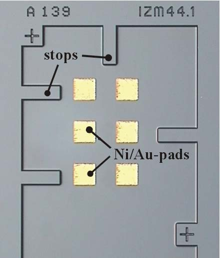 | |
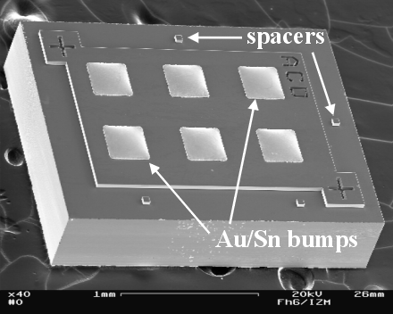
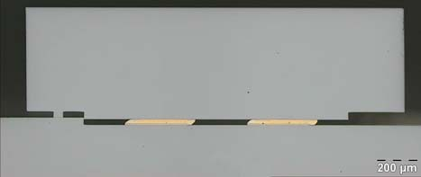
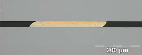
| Figure 1: Photograph of a Si test substrate with Ni/Au pads. | Figure 2: SEM photograph of a Si test die. Stops were etched using Reactive Ion Etching. The AuSn bumps on the die were reflowed after electroplating |
As the restoring forces during self-alignment are proportional to the misalignment the pads on the substrate and bumps on the chip are still purposely not arranged in full opposition when the stops are in contact to each other. In addition to effectively utilize the restoring forces the chip is placed on the substrate such that there is a misregistration between bumps and pads of approximately 100 µm prior to soldering. This huge misregistration was chosen in order to have a better chance to overcome the interfacial friction forces among the mechanical stops. In other words, the concept pursued uses misaligned solder joints and mechanical stops.
You can download the Project files here: Download files now. (You must be logged in).
Substrate Preparation
One of the problems which had to be solved is the deposition of resist on wafers with deep etched cavities (40 µm) which has not been a standard process step. For this reason different techniques were investigated for the coating of wafers with strong topology. Optimization led to different processes for small (15 µm) plating structure heights. The thin resist was achieved by specially tuned multiple spray coating of Novolac resist. The thick resist was coated in a multiple spin coating process using Novolac resist of different viscosity and adapted baking steps. Both processes result in bubble free and step covering layers on strong topology wafers. A resist thickness range from 2 µm to approximately 40 µm could be covered.
On the substrate wafers Ni/Au pads were deposited using electroplating of 5 µm thick Ni pads and sputtering for the 200 nm thick Au finish. The substrates are designed such that the Ni/Au pads sit in 40 µm deep etched cavities. In Figure 1 a photograph of a test substrate is shown. There are 6 Ni/Au pads surrounded by 4 stops acting as spacers and crosses acting as alignment marks in the corners.
Chip Preparation
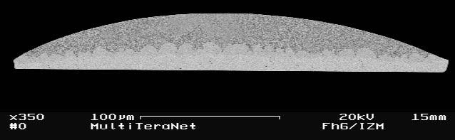
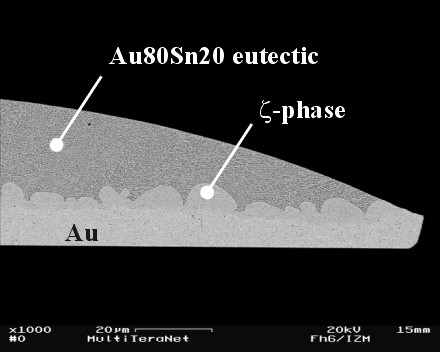
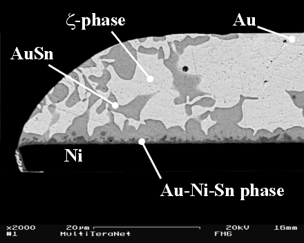
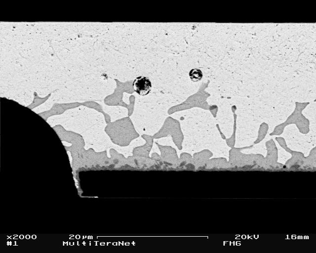
The solder bumps were deposited on the chip wafers. Eutectic Au80Sn20 solder was used because it allows fluxless flip chip assembly which is mandatory for optoelectronics packaging in order to prevent the optical interface from contamination. The Au/Sn bumps have been manufactured by electroplating of Au and Sn in successive process steps followed by a reflow in liquid medium which is necessary to form the eutectic solder cap on top of the bumps (Figure 2). After the reflow process had been accomplished these Au/Sn bumps consist of a Au layer with a solder cap on top consisting of 80 wt.-% Au and 20 wt.-% Sn forming the eutectic microstructure. In between the eutectic cap and the Au pedestal the intermetallic phase Au5Sn (z-phase) has been formed. SEM micrographs of cross sections of Au/Sn bumps after electroplating and reflow are shown in Figure 3 and Figure 4. The electroplating process as well as the reflow process including the phase transformations during the reflow have been described in detail elsewhere2, 5, 6. To ensure a satisfactory reflow result the bumps were aged at elevated temperature, i.e. 200 °C for 4 hours, prior to the reflow. Applying this pretreatment the phase transformation during the reflow process can be controlled very well.
The shape of the bump, i.e. the height of the total bump and the thickness of the eutectic cap as well as the height of the remaining Au layer beneath the eutectic solder cap, was carefully adjusted by calculating the heights of the Au and Sn layers deposited. In previous work it has been shown that it is possible to predict the shape of the Au/Sn bumps using the volume equation of cut spheres5. Applying this calculation a Au layer of 17 µm and a Sn layer of 7 µm thickness were plated, i.e., the total thickness of the bumps as plated was 24 µm. This leads to a calculated bump height of 38 µm after reflow consisting of a remaining Au layer of 5 µm, a z-phase layer thickness of also 5 µm and a eutectic cap on top of the bumps of approximately 28 µm in height. The cross sections shown in Figure 3 and in Figure 4 reveal that the cap height achieved as well as the thickness of the z-phase and the thickness of the remaining Au layer fit well to the calculation.
An SEM micrograph of a test chip after electroplating the Au/Sn solder bumps and reflow them is shown in Figure 2. This test chip has 4 stops as to determine the stand off of 50 µm * 50 µm area which had been etched 10 µm deep in the original Si surface. The test chip also has two crosses as alignment marks so that the assembly process can be tested with automatically operating pick & place equipment.
Flip Chip Assembly
The flip chip assembly was done by pick and place and reflow above 280°C. The placement was performed using a flip chip bonder. In Figure 5 it is shown how the substrate and the chip were aligned before assembly. The soldering process was carried out in an oven in activated atmosphere. After placement but prior to soldering the chip was tested to be in the right position using Infrared (IR) microscopy. Figure 6 shows an IR microscope image of a chip which was placed on the substrate. The bumps and pads are intentionally misregistered to each other to approximately 100 µm. The liquid tacking medium which prevents the chip from movement during carrying the pre- assembly to the reflow oven is also visible on the substrate pads. The tacking medium completely disappears when the assembly is heated above the melting point of the eutectic Au80Sn20 solder of 280 °C and therefore does not cause any contamination on the optically active surfaces.
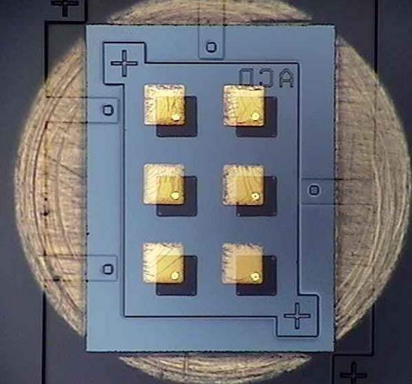 | 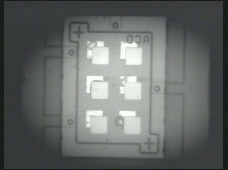 | |
| Figure 5: Superpositioned view from bonder: chip with AuSn bumps and substrate with Ni/Au pads | Figure 6: Infrared microscope image of a Si chip which was aligned to a corresponding Si substrate. | |
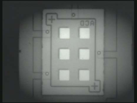 | 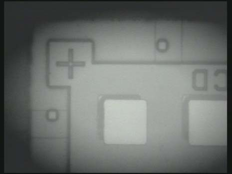 | |
| Figure 7: Infrared microscope image of the assembly after the soldering process was carried out. | Figure 8: Detailed picture of Figure 7 | |
Figure 7 shows an IR image of the same sample after reflow soldering was performed and Figure 8 a magnification. The chip moved until it was stopped by the mechanical stops. Although the resolution of the IR microscopy is insufficient to prove whether or not the required alignment accuracy was achieved it is a suitable means of showing that the chip has moved towards the stops and is at least very close to its desired position. It can also be seen that there is still a distortion of the solder bumps after the chips moved towards the stops.
You can download the Project files here: Download files now. (You must be logged in).
 |  | |
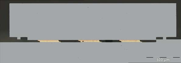
| Figure 9 Left: Cross-sectional view of a flip chip assembly. Right: Enlarged view on displaced bump interconnect providing alignment force. | ||
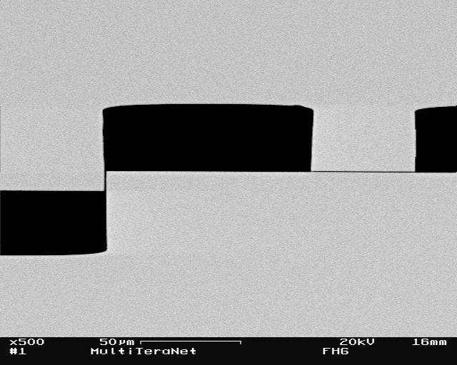
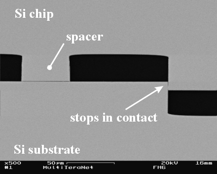 | Cross-sections in Figure 9 reveal the aligned flip chip with the stops and the remaining solder bump distortion which was applying a force to the stops before solidification. Cross sections in Figure 10 through the stops reveal that they are in direct contact with the corresponding silicon surface. The standoffs as well as the etched Si structures are in direct contact. Therefore it is possible to achieve high precision alignment which is solely determined by the mechanical stops or standoffs in at least two directions. As the third direction is parallel to the optical axis the alignment accuracy in this direction is in the order of only 5 µm. The IR images show that the chip also moved in the direction parallel to the optical axis and that the movement of the chip is also stopped by the corresponding stop surfaces. Figure 13 and Figure 14 are representing the AuSn solder joints which have wetted the nickel pads very well. | |
| Figure 10: Cross section SEM image of a flip chip assembly.The stops are in direct contact with each other. | ||
 |  | |
| Figure 11: Cross section light microscope image of a flip chip solder joint. | Figure 12: Cross section SEM image of a flip chip solder joint. | |
In Figure 13 another type of stop is shown which extends along the full side. The successful self-alignment can be recognized in the cross-section in Figure 14 where the enlarged bump structure is visible. The mechanical stop is presented in detail in Figure 15. There is a very small gap between the stop and the corresponding edge visible which is around 1 µm. This might be an indication, that mechanical stops of small dimension are favored over extended stop types.
 |  | |
| Figure 13: IR image of self-aligned flip chip assembly with long stops. | Figure 14: Cross-sections self-aligned chip assembly of Figure 13 (top) and enlarged view on AuSn bump (bottom). | |
 |  | |
| Figure 15: Enlarged view on mechanical stops of self-aligned chip assembly in Figure 14 (top). | Figure 16: SEM picture of solder joint from assembly in Figure 14. AuSn solder joint well to Ni pads. | |
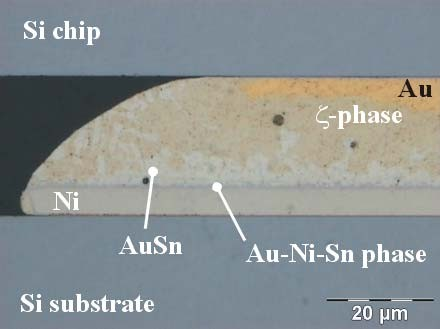
The flip chip interconnects have also been investigated. A light microscope image of a solder joint is shown in Figure
- It can clearly be seen that there is still an attractive arrangement of more than 30 µm left between the bump’s Au layer and the Ni pad on the substrate even though the chipmoveduntil it was stopped by the mechanical stops and the stops are in direct contact to each other. In Figure 12 as well as in Figure 16 the SEM image clearly shows the well wetting on the Ni pads. Intermetallic phases which formed during soldering are visible. Due to the dissolution of some nickel in the solder the microstructure becomes coarse compared to the pure eutectic composition of the Au/Sn solder bumps. The solder joint still consists of the intermetallic phases AuSn and Au5Sn (z-phase).
You can download the Project files here: Download files now. (You must be logged in).
Conclusions
A concept for passive alignment was presented. In order to prove that this concept is viable test vehicles were designed and fabricated. It has been shown that it is possible to deposit Au/Sn solder and Ni pads by electroplating on wafers of a special etched topology which was created by Reactive Ion Etching.
First flip chip assembly tests have shown that it is possible to use the self-alignment mechanism in combination with mechanical stops. The chip moves until it is stopped through the stops, i.e., the final position of the chip in regard to the substrate is determined solely by the stops.
In conclusion, the proposed passive alignment flip chip assembly technique successfully integrates the self-alignment properties of liquid solder with the precision control of micromechanical stops, offering a robust and low-cost alternative to traditional active alignment. Experimental results from silicon test vehicles validate that submicron alignment accuracy is achievable through the synergistic interaction between surface tension forces and mechanical constraints. This approach significantly reduces assembly complexity, enhances reproducibility, and paves the way for scalable, automated production of optoelectronic components. The developed methodology holds great potential for future integration in laser diode packaging, photonic integrated circuits, and optical interconnect systems, where high precision, reliability, and cost efficiency are paramount.
References
1 Tan, Q., Lee, Y.C., “Soldering Technology for Optoelectronic Packaging”, Proc 46th Electronic Components and Technology Conf, Orlando, 1996.
2 Kallmayer, C., Oppermann, H., Kloeser, J., Zakel, E., Reichl, H., “Experimental Results on the Self-Alignment Process Using Au/Sn Metallurgy and on the Growth of the z–Phase During the Reflow,” Proc International Flip Chip, Ball Grid Array, TAB and Advanced Packaging Symposium, ITAP’95, San Jose, 1995.
3 Rehm, W., et al., “Low Cost Laser Module for SMT” Proc 50th Electronic Components and Technology Conf, Las Vegas, 2000.
4 Renaud, M., et al., “SOA-based Optical Network Components”, Proc 51st Electronic Components and Technology Conf, Orlando, 2001.
5 Hutter, M., Oppermann, H., Engelmann, G., Wolf, J., Ehrmann, O., Aschenbrenner, R., Reichl, H., “Calculation of Shape and Experimental Creation of AuSn Solder Bumps for Flip Chip Applications,” Proc 52nd Electronic Components and Technology Conf, San Diego, 2002.
6 Dietrich, L., Engelmann, G., Ehrmann, O., Reichl, H., “Gold and Gold-Tin Wafer Bumping by Electrochemical Deposition for Flip Chip and TAB,” 3rd European Conference on Electronic Packaging Technology (EuPac’98), Nuremberg, Germany, June 15-17, 1998.
You can download the Project files here: Download files now. (You must be logged in).


Responses