

Advanced Concepts for Edge Emitting Light Source to Photonic Integrated Circuit Coupling
Author: Waqas Javaid
Abstract—This study emphasizes the pivotal role of Edge- Emitting Lasers (EELs) within Photonic Integrated Circuits (PICs), highlighting their superior beam quality and higher output power for effective optical coupling and integration. Addressing the connection challenges in PICs, Die-to-Wafer (D2W) bonding is spotlighted as a crucial technique for aligning semiconductor devices like EELs with CMOS sensors. The study demonstrates D2W bonding’s adaptability and its profound impact on performance, scalability, and integration of photonic components. EELs, with their high radiance and narrow beam divergence, are shown to be more suitable for high-output ap- plications compared to Vertical-Cavity Surface-Emitting Lasers (VCSELs). The research also underlines the importance of precise alignment in D2W bonding, dictating an alignment tolerances of 5.5 µm in the vertical and lateral axes, to ensure a 94 percent butt coupling efficiency,effectively resolving the size mismatch problem.
Index Terms—Edge-Emitting Lasers (EELs), Photonic Inte- grated Circuits (PICs), Die-to-Wafer (D2W) Bonding, Optical Coupling.
- Introduction
HOTONIC Integrated Circuits (PICs) are an emerging modern data transfer and sensor technology, extending their transformative potential to a plethora of applications such as medical diagnostics, chemical sensing, high-speed data transmission, light detection and ranging (LiDAR), distance metrology, and ultra-broadband signal processing applications [1]. The success of this technology is mainly attributed to the low cost, robust performance, low power consumption, and scalability of the photonic devices [1], [2], [3]. Silicon, the main component in these photonic devices, can be used to construct compact devices. This is due to its high refractive index and the fact that silicon-based devices tend to be compatible with the current mature and standardized Complementary Metal Oxide Semiconductor (CMOS) platform [4].
Despite these advances, the commercial application of PICs faces formidable challenges, especially in achieving precise chip-to-chip and fiber-to-chip connections. In these connec- tions (also known as butt coupling), the facets of the devices to be connected are brought in close proximity, or a physical direct connection (contact) between the devices is achieved. However, this approach needs high-precision active alignment with sub-micrometer accuracy [1]; hence, the risk of error during the process is considerably high. Additionally, the size mismatch between silicon-based waveguides on the nanometer scale and the much larger diameter of a standard single-mode fiber (SMF) – approximately 125 µm with a core diameter of about 10 µm – poses a significant challenge. This discrepancy can lead to substantial optical transmission losses if light from the fiber enters directly into the Si waveguide [4].
To address these complexities, Die-to-Wafer (D2W) bond- ing has emerged as an indispensable technique in photonics. It facilitates the alignment and integration of semiconductor devices, such as light sources and CMOS sensors, onto a unified wafer. The D2W bonding process, utilizing advanced pick-and-place flip-chip bonders, is critical for assembling in- tricate photonic devices and creating highly compact, efficient, and high-performance photonic modules. The importance of D2W bonding is further emphasized by its profound impact on photonic components’ performance, scalability, and inte- gration. This technique is mainly instrumental in overcoming the challenges associated with the hybrid integration of devices like edge-emitting lasers (EELs) and CMOS sensors, ensuring optimal alignment and bonding that is essential for the en- hanced functionality and performance of photonic circuits [1], [3], [5], [6].
D2W bonding’s adaptability is showcased in its application to Vertical-Cavity Surface-Emitting Lasers (VCSELs) and Edge-Emitting Lasers (EELs), integral components of the photonics landscape. Due to their surface-normal emission, VCSELs are extensively employed in data communication and sensing applications. EELs, known for their edge emission, are essential for high-power optical transmission. The hybrid D2W bonding approaches, such as eutectic and adhesive bonding, provide tailored solutions that enhance these lasers’ perfor- mance, reliability, and integration efficiency within photonic devices [1].
The emphasis on EELs in this research is driven by their superior beam quality and higher output power, which are beneficial for efficient optical coupling and integration into photonic circuits [1]. These attributes of EELs are indispens- able for high-performance and reliable applications, justifying their focused study in the context of D2W bonding and photonic packaging. The alignment tolerances in the D2W bonding process are critical parameters that dictate the allow- able deviations in component positioning to ensure optimal device performance [1], [3], [5], [6].
2. Die-to-wafer(D2W) bonding
Die-to-wafer (D2W) bonding has emerged as a pivotal tech- nique in the semiconductor industry, particularly for the inte- gration of light sources, such as edge-emitting lasers (EELs), with complementary metal-oxide-semiconductor (CMOS) sen- sors. As technology advances, moving away from traditional macroscopic gluing layers [7], which provide adherence to different materials at room temperature, has led to the development of more sophisticated bonding methods. These

- Fig. 1. Eutectic Bonding [9]
methods, such as eutectic and adhesive bonding, are tailored to meet the specific needs of hybrid D2W bonding, where dies are meticulously placed onto the final wafer using precise equipment like pick-and-place flip-chip bonders [8].
A. Eutectic Bonding
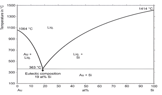
Eutectic bonding relies on creating a eutectic system, where a specific composition of metals can melt at a singular eutectic temperature. In the case of EELs, the Au-Sn (gold-tin) system is prevalently used due to its favorable eutectic temperature of around 280 degrees Celsius, which is suitable for many 3D wafer bonding applications. This system facilitates a clean transition from solid to liquid phase without the coexistence of the two, which is crucial for creating a reliable bond without the need for high temperatures that could damage sensitive semiconductor devices. As depicted in Figure 1, the eutectic composition at 19 at% Si demonstrates the precise melting point required for such bonding [9].
This method involves depositing a single alloy layer using electroplating, dual-source evaporation, or composite alloy sputtering techniques. During the bonding process, the alloy is melted at the eutectic point and then reconsolidated, forming a strong bond between the dies and the wafer. The process often operates at a slightly higher temperature, around 290 degrees Celsius, to decrease the viscosity of the melt and ensure it fills any surface irregularities, enabling it to accommodate surfaces that are not perfectly smooth without exerting excessive force, which could misplace the material. The adaptability of this process is further illustrated by the possibility of layering pure gold and pure tin on separate wafers, which, upon heating, allows for tin melting and gold diffusion, creating a robust interface [10].
B. Adhesive Bonding
Adhesive bonding, however, provides a broader application scope due to its flexibility, particularly in scenarios involving incompatible materials or stringent temperature constraints that eutectic bonding cannot meet. This method uses an intermediary adhesive layer to bond the die to the CMOS chip. Adhesives such as glass, epoxies, photoresists, and other poly- mers can be employed, depending on the requirements of the substrate and application. For instance, glass frits can be used with sealing temperatures ranging from 400 to 650 degrees Celsius, which melt and flow upon annealing to create a seal once cooled to room temperature. The versatility of adhesive

- Fig. 2. Adhesive Bonding [10]
bonding is such that it can be applied to many materials and is not limited to silicon, making it an invaluable technique in the microelectronics field [11]. The SU-8 photoresist is a notable example, acting as both a spacer and an adhesive layer in microfluidic applications, capitalizing on the low process temperatures required by polymers, which are beneficial for devices with low melting point metals and alloys [8], [9].
The choice between eutectic and adhesive bonding depends on several factors, including thermal budget, material compat- ibility, and the required precision in alignment [12]. Eutectic bonding’s precision and reliance on a defined melting point are advantageous for its self-alignment properties and the strength of the metallic bond formed. However, its application is limited by the thermal tolerance of the materials involved. Adhesive bonding, with its lower temperature requirements and adaptability to various substrates, provides a solution for materials that cannot withstand the higher temperatures of eutectic bonding. Furthermore, adhesives accommodate a broader range of topographical variances and can provide additional functionalities, such as electrical insulation or me- chanical cushioning.
3. Hybrid Die-to-Wafer (D2W) Bonding
Hybrid Die-to-Wafer (D2W) bonding is emerging as a trans- formative technique for packaging photonic integrated circuits (PICs), significantly enhancing commercial scalability. The method addresses the alignment challenges between fibers and PICs, facilitating efficient connections. Plasma-assisted D2W molecular bonding has been particularly examined for its effectiveness in integrating edge-emitting lasers, such as hybrid silicon lasers, onto silicon-based PICs, which could lead to high-yield multiple die-to-wafer bonding, crucial for large-scale production.
Kostrzewa, et al. [13] demonstrated the feasibility of molec- ularly bonding indium phosphide (InP) dies, as small as 1 mm by 1 mm, to a 200 mm silicon CMOS wafer. Their process involved covering both wafers and dies with an oxide layer to facilitate a strong hydrophilic bond and employing pick-and- place technology for precision in alignment and application of mechanical force. However, Van Campenhout, et al. [14] noted that despite the successful integration of electrically pumped

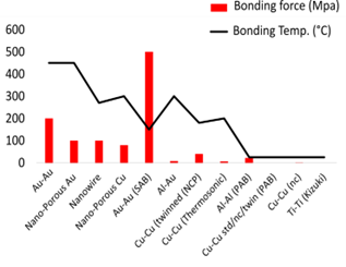
- Fig. 3. Comparison of bonding temperature and bonding force associated with various hybrid D2W bonding techniques
microdisks with silicon waveguide circuits, contamination on the bonding surfaces could occur during cleaning, potentially affecting the bonding yield and quality. Moreover, the lengthy bonding time of approximately one hour for 100 dies could lead to the deactivation of the bonding surfaces.
Luo, et al. [5] and Stankovic´, et al. [15] suggest that Bis- benzocyclobutene (BCB) adhesive bonding can circumvent die number and speed limitations. It involves spin coating a silicon wafer with a thin BCB layer, followed by die attachment and curing at about 240°C. This technique is less stringent on surface smoothness and contamination control, thus potentially enabling larger-scale manufacturability [16]. However, while BCB bonding is robust and offers high strength, its major limitation is poor thermal dissipation due to the low thermal conductivity of the BCB layer, which could lead to damage if not properly managed [5]. Roshanghias, et al. [17] highlighted the relationship between stage temperature and interface tem- perature, emphasizing the importance of enhancing thermal conductivity to prevent damage.
Metal-assisted adhesive bonding has also been considered for hybrid laser integration, but it carries risks of metal contamination and compatibility issues with subsequent fab- rication processes, such as acid etching [5]. Further studies by Roshanghias, et al. [17] and Jouve, et al. [18] explored thermosonic flip-chip bonding of copper pillars and copper interconnections in D2W bonding, respectively. Both studies support the potential of D2W hybrid bonding for the commer- cialization of silicon-based photonics due to enhanced bond strength. The attached figure correlates bonding temperature with various materials and techniques. It indicates that, gener- ally, higher bonding temperatures result in greater bonding forces, except for the Au-Au (SAB) hybrid. This suggests a significant impact of temperature on the bonding force in hybrid bonding techniques.
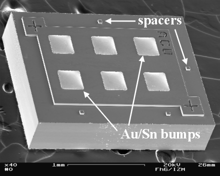
4. Passive Alignment Flip-Chip Assembly
The passive alignment technique for flip-chip assembly presents an innovative approach to optoelectronic packaging, significantly reducing costs while achieving high precision [19], [20]. This method harnesses the self-alignment capa- bilities from surface tension and mechanical stops generated by molten (liquid) Au/Sn solder, eliminating the need for

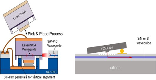
- Fig. 4. An illustration of the coupling of edge-emitting lasers, EEL (Left), and coupling of vertical cavity surface emitting lasers, VCSEL (Right) [21]
active alignment. The process begins with the intentional misalignment of the solder bumps and substrate pads, typically by about 100 µm. During reflow, which occurs above the solder’s melting point of 280°C, the surface tension of the liquid solder corrects this misalignment, pulling the chip into its correct position against the mechanical stops designed into the substrate. This method has proven effective, with alignment accuracy better than 2 µm, showcasing its potential for applications requiring high precision without the associated high costs of active alignment methods.
A passive alignment process was demonstrated using test vehicles made of silicon, where Au/Sn solder and Ni pads were deposited through electroplating, followed by Reactive Ion Etching to create the required stops for alignment [20]. Infrared (IR) microscopy was employed pre- and post-reflow to assess the chip’s positioning relative to the substrate. An analysis of the results produced by Oppermann et al. [20] confirms that the chip moves towards the mechanical stops, achieving a final position very close to the desired alignment. Cross-sectional views further substantiate that the mechanical stops directly contact the silicon chip, ensuring precise alignment.
The passive alignment technique is cost-effective and min- imizes the risk of contamination since the liquid tacking medium used during pre-assembly completely evaporates dur- ing reflow. Additionally, this method does not adversely affect the optically active surfaces, as evidenced by the absence of contamination post-reflow. Furthermore, the SEM images from Oppermann et al.’s [20] report reveal well-wetted solder joints, indicating strong and clean interconnections. However, it’s noteworthy that while the mechanical stops are effective, their size and placement are critical, as indicated by the slight gap (approximately 1 µm) observed in some instances.
You can download the Project files here: Download files now. (You must be logged in).
5. The Superiority of EELS Over VCSELS
The integration of light sources into silicon-based photonic integrated circuits necessitates a meticulous selection of ac- tive materials and integration techniques due to the inherent inefficiency of silicon emitters. Among the strategies, edge- emitting lasers (EELs) and vertical-cavity surface-emitting lasers (VCSELs) represent the most mature technologies for integrating silicon nitride waveguides.
EELs, employing in-plane coupling, offer a robust solution with their light propagation in the same plane as the

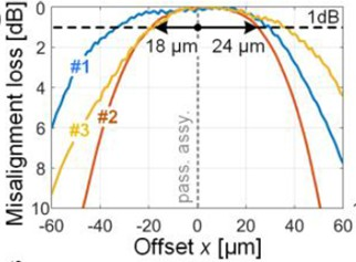
- Fig. 5. The effect of misalignment and spatial alignment [1]

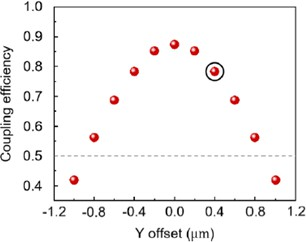
- Fig. 6. The effect of spatial alignment (offset) on coupling efficiency [22]
waveguide. This method is characterized by low insertion loss, rendering it highly efficient and wavelength-independent. Such attributes are crucial for applications demanding high throughput and reliability. The spatial alignment and chip geometry, albeit demanding in precision, contribute to the effective coupling of the EELs to the waveguides, as evidenced by the direct correlation between misalignment loss and offset depicted in the associated figures.
In contrast, VCSELs operate with vertical resonant cavities, wherein the light oscillates perpendicular to the active layers. The configuration of VCSELs allows for greater alignment tolerances, facilitating easier fabrication processes. However, this comes at the cost of reduced overall gain due to the limited dimensions of the cavities and the thinness of the active layers. The performance of VCSELs is inherently wavelength and polarization-dependent, factors that can constrain their utility in a broad range of applications. The intricate relationship between etch depth and device efficiency, as well as the polarization angle and efficiency, has been well-documented and underscores the intrinsic limitations of VCSELs [1].
EELs offer a superior integration strategy. The lower insertion losses and independence from wavelength variability confer upon EELs a distinct advantage in performance. While the meticulous requirements for spatial alignment and precision in chip geometry preparation present manufacturing challenges, the resulting efficiency gains substantiate the investment in EEL technology. In large-scale commercial production, these challenges are non-trivial yet offset by the enhanced performance and efficiency of EELs.
Thus, adopting EELs for light source integration into PICs is advocated despite the complex alignment and preparation pro- cesses. The consistent performance and efficiency advantages of EELs substantiate their selection as the preferred technology for PIC integration, a conclusion drawn from a comprehensive analysis of their operational characteristics and efficiencies. The ongoing advancements and enhancements in both EEL and VCSEL technologies will continue to refine their applications. Still, the current state of technology positions EELs as the more advantageous choice for scalable, efficient PIC integration.
6. Experimental and Simulation Analysis of EELS
In this section, we delve into the integration of Fabry-Perot Edge Emitting Lasers (EELs) with Si3N4/SiO2 Rib-loaded waveguides (RIB waveguides) on silicon substrates, a critical component in the development of efficient photonic systems for applications such as communication, signal processing, optical sensors, and photonic integrated circuits [23], [24], [25], [26], [27], [28], [29]. The Si3N4/SiO2 waveguides, with Si3N4 as the core material and SiO2 as the cladding material, offer a large transparent spectrum and ultra-low propagation loss, making them ideal for such applications [24], [25]. A significant challenge in this integration is the efficient coupling of light from the EELs into the RIB waveguides, par- ticularly due to the size mismatch between the fiber core and the silicon waveguide in chip-to-fiber connections. To address this, we explore a fiber-to-waveguide coupler implemented on the Si3N4/SiO2 waveguides [29]. This coupler boasts an ultra-high coupling efficiency of 98% in theory and 96% in experiments [29], along with an ultra-broadband transmission spectrum, ease of cleaving, and large alignment tolerances. The design and implementation of this coupler are pivotal in achieving efficient light transfer between the EELs and the RIB waveguides.
Three major approaches are widely adopted for coupling: grating couplers (GCs), taper-based couplers, and evanescent- field coupling. While commonly used, grating couplers offer limited bandwidth and require a subsequent mode-converter for single-mode operation [30], [31], [32]. Taper-based couplers provide a broader bandwidth solution but necessitate precise end-facet cleaving [33]. Evanescent-field coupling, involving an overlap region between a conical tapered fiber and a tapered waveguide, shows promise for efficient coupling but poses challenges for large-scale integration [34].
In this analysis, we conduct both experimental and simulation studies to evaluate the coupling efficiencies of these approaches, with a particular focus on the fiber-to-waveguide coupler implemented on Si3N4/SiO2 waveguides. The results aim to provide comprehensive insights into the optimal coupling strategies, facilitating the development of more efficient and integrated photonic systems. The approach introduced here

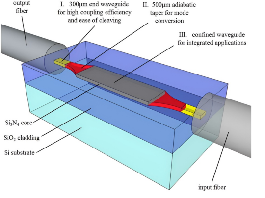
- Fig. 7. Si3N4/SiO2 waveguide coupler design adopted from Zhu, et al. [29]
also applies to multi-device operations, further enhancing the versatility and scalability of the photonic integration platform.
A. Design and Modeling
1) Waveguide Coupler Design: The Si3N4/SiO2 waveguide coupler design, as depicted in Figure 7, employs a three-part structure to optimize fiber-to-waveguide coupling on a silicon substrate. The primary borrowed concept is the use of a Si3N4 core and SiO2 cladding, which, compared to SOI platforms, provides transparency across a broader spectrum – from the visible to the near-infrared – offering particular advantages for sensor and astronomy applications due to this extended operation range [35], [36].
In the original design, Part I is a 500 µm segment of loosely- confined straight waveguide tailored for ultra-broadband coupling efficiency. This section is engineered to permit significant tolerance in the cleaving position, allowing a ±200 µm variance without compromising coupling efficiency, thus addressing the precision cleaving challenge seen in taper-based couplers. Part II, a 500 µm adiabatic taper, ensures gradual mode conversion with minimal loss. In contrast, Part III, a 300 µm confined waveguide, is the integration bed for various photonic structures like waveguide Bragg gratings and ring resonators.
The modification introduced in our design involves restructuring Part I into a Rib-waveguide configuration with a precise etch depth of 5 µm. This adaptation significantly increases the vertical confinement of the optical mode due to the deeper etch, which in turn enhances coupling efficiency with the fiber. The Rib structure provides a more definitive boundary between the core and cladding layers, improving the phase-matching conditions with the fiber mode and, thus, the overall coupling efficiency. This theoretical improvement is supported by the fact that a deeper etch depth in the Rib-waveguide enhances the overlap of the evanescent field with the fiber mode, which is critical for efficient power transfer.
In analyzing our photonic coupler design, Ansys ZEMAX OpticStudio, supplemented by the Physical Optics Propagation (POP) plugin, served as our simulation platform [37]. This optical simulation software provides the capability to rigor- ously model light propagation from a commercial Fabry-Perot (FP) laser diode, capturing the wave behavior as it traverses through different media. We performed our initial simulations
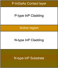
TABLE I: Fabry-Perot Laser Diode Parameters
Layer | Material | Thickness (µm) |
Substrate | Indium Phosphide (InP) | 6.0 |
N-doped (Lower) Cladding | Indium Phosphide (InP) | 1.0 |
Active Region (5 stack QW) | – | – |
– Barrier | AlGaAs x=0.198 (Aspens) | 0.008 |
– Quantum Wells | InGaAs | 0.01 |
P-doped (Upper) Cladding | Indium Phosphide (InP) | 0.85 |
Contact Layer | P-doped InGaAs | 4.5 |
on Ansys Lumerical Mode solutions to determine the mode profiles emanating from the FP laser diode accurately. The output from this stage was then seamlessly integrated into ZEMAX for comprehensive POP analysis. This approach ensured that the virtual light’s propagation from the laser diode, through the coupler, into the waveguide is modeled with high precision, reflecting real-world performance with fidelity.
The integration of simulation outputs from Lumerical Mode into ZEMAX OpticStudio and back into Lumerical’s Finite- Difference Time-Domain (FDTD) environment for Time- Dependent analysis establishes a robust feedback loop that enriches our understanding of wavelength variations across the 1400 nm to 1600 nm range. This meticulous simulation workflow enables us to fine-tune our design to ensure optimal performance across a broad spectrum, which is pivotal for applications in telecommunications and sensing. The choice of Ansys’ tools, with their established reputation for accuracy and versatility, provides a solid justification for their use in our simulation studies, reinforcing the credibility and reliability of our findings.
You can download the Project files here: Download files now. (You must be logged in).
B. Fabry-Perot Laser Design
Utilizing a 1550 nm Fabry-Perot laser diode crafted from InGaAlAs/InP for enhanced clarity and precision showcases substantial efficacy in PIC simulations and edge coupling integration. The laser’s active region integrates a strain- compensated multi-quantum-well design, yielding superior optical confinement and gain characteristics. Central placement within the graded index separate confinement heterostructure (GRIN-SCH) biases the laser mode distribution towards the n- type cladding. This strategic bias minimizes mode overlap with the p-type doped cladding, effectively reducing internal optical loss and increasing semiconductor laser output power [38]. The selection of InP for the substrate and cladding, coupled with InGaAs for the quantum wells, ensures a high degree of lattice matching and robust carrier confinement, pivotal for the laser’s radiative efficiency and consistent performance at the crucial 1550 nm near-infrared wavelength. The design is further optimized by employing a high numerical aperture UHNA3 fiber with a minimal mode field diameter of 4.1 µm at 1550 nm, enhancing the interface with the waveguide coupler. This setup ensures a low splice loss with standard single-mode fibers, such as the SMF28.

- Fig. 8. Schematic representation of modeled Fabry Perot Semiconductor laser

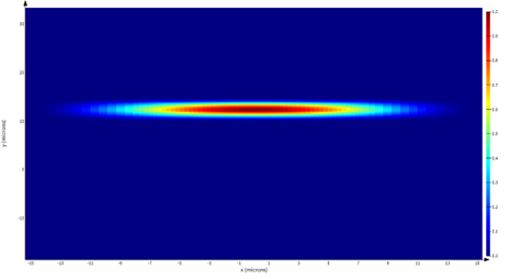
- Fig. 9. Normalized TE fundamental propagating mode pumped at 1.55 µm / 50 fs wavelength from the FP semiconductor laser.
7. Results and Discussion
A. Simulation Results
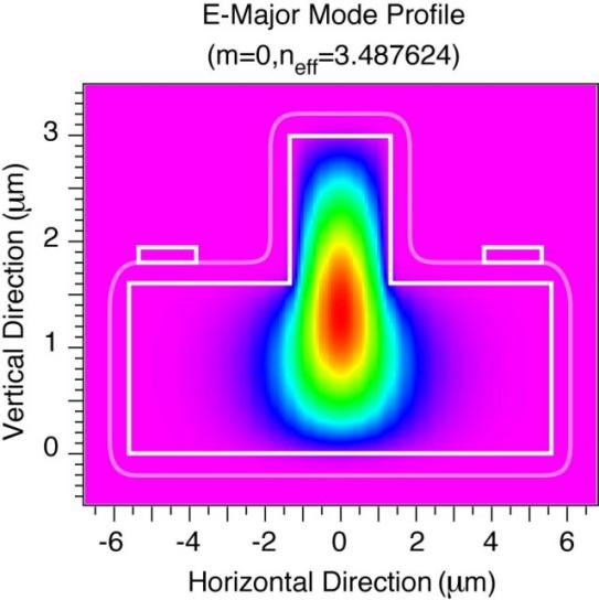
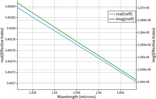
The effective index plot exhibits a steady real component with a slight downward trend, indicating stable mode confinement over the wavelength range. At the same time, the near-flat imaginary part suggests low modal absorption. The mode intensity profile confirms effective light confinement, with the highest intensity at the center, crucial for strong laser action. The loss graph displays an increment in loss as wavelength increases, a normal behavior for semiconductor lasers, and remains under 3.6 dB/cm, indicating a well-optimized waveguide with controlled scattering and absorption losses.
B. Influence of Variation of Geometrical Parameters on Waveguide Parameters
The study of waveguide geometry is crucial as it impacts chromatic dispersion. Varying geometrical parameters is important to achieve high nonlinearity and low dispersion (almost flat curves) in the design. Errors in waveguide fabrication can alter dimensions. Geometrical parameters (such as etch depth and width) affect the effective group refractive index, which decreases with longer wavelengths (>1550 nm) due to faster light velocity. Core width changes have minor effects, while core height and core maximum height changes significantly

- Fig. 10. Effective Index plot indicating stable mode confinement over the central 1550 nm wavelength range

- Fig. 11. Transverse cross-section of rib waveguide with parameters (Core Width – a, Core Trench Height (or etch depth) – b, Core Maximum Height – h, Waveguide Width – w)
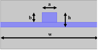
influence the refractive index [39]—a lower effective refractive index results in higher mode velocity, and vice versa. Core width and maximum height effectively increase refractive index across all wavelengths, whereas core height decreases it. The impact is more pronounced at higher wavelengths for core height and core maximum height. Furthermore, the effective mode area represents the mode’s propagation space within the waveguide. We observe that the core width and core maximum height have minimal influence, while core height strongly affects the effective mode area. Interestingly, increasing core width decreases effective area throughout the wavelength range. Increasing core trench height significantly increases mode area at higher wavelengths. All these results have been adequately documented in the works of Sharma, et al. [39], and our experimental results similarly showed a strong correlation and agreement with their findings at 1550 nm wavelength.
C. Coupling Efficiency and Alignment Tolerance Investigation
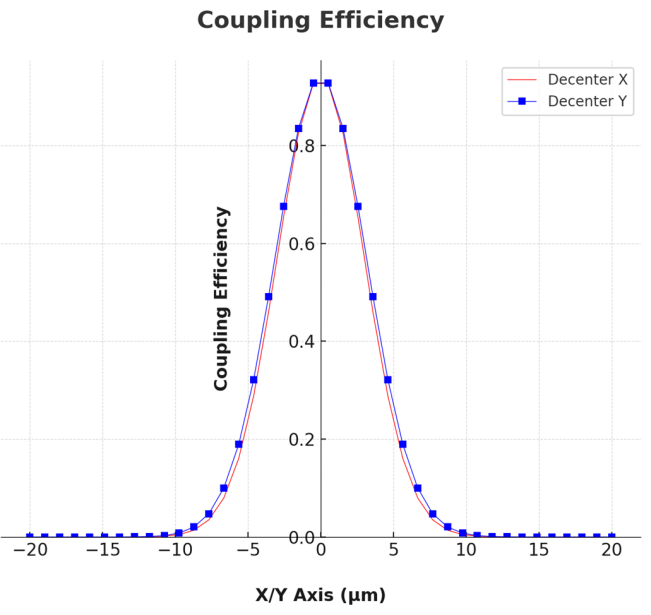
The simulation data depicted in Figure 13 presents the calculated coupling efficiencies as a function of lateral misalignment in both the X and Y axes. The peak coupling efficiency is observed at the center of the optical axis, sharply decreasing as the lateral misalignment increases. The maximum coupling efficiency, 94%, signifies an excellent concentration of optical power in the waveguide. The Decenter X and Decenter Y lines follow a similar trend, suggesting a symmetric response to

- Fig. 12. E-intensity (TE-mode) Mode Profile across rib-waveguide
TABLE II
Theoretical and Experimental Alignment Tolerances Between the UHNA3 Fiber and the Si3 N4 /SiO2 Waveguide
Simulation Data | Experimental Data | |
Horizontal Direction Vertical Direction | 5.6 µm 5.5 µm | 5.8 µm 5.6 µm |
misalignment in the horizontal and vertical directions, which is desirable for uniform fabrication tolerances.
The consistency of the X and Y axes implies an isotropic behavior of the waveguide’s refractive index or the mode field diameter of the laser being used. The steep drop-off in efficiency beyond the ±5 µm range is notable. It suggests that the alignment tolerances for the optical components need to be tightly controlled during the packaging process to ensure optimal performance.
Table II compares the theoretical and experimental alignment tolerances between the UHNA3 fiber and the Si3N4/SiO2 waveguide. The data reveals a close agreement between simulation and experimental results, with the horizontal direction showing a tolerance of 5.6 µm in simulations and 5.8 µm experimentally. Similarly, in the vertical direction, the simulation predicts a tolerance of 5.5 µm while the experimental value is slightly higher at 5.6 µm. This near-congruence validates the simulation model and suggests it can be a reliable predictor of real-world outcomes.
The experimental data underscores the precision required in the alignment process, as even minor deviations can lead to significant losses in efficiency. The tight tolerance also emphasizes the need for advanced fabrication techniques, such as precision dicing or laser welding, which can maintain alignment within the required tolerances.
8. Conclusion and Recommendation
A. Conclusion
The integration of Edge Emitting Lasers (EELs) with Si3N4/SiO2 Rib-loaded waveguides (RIB waveguides) on silicon substrates represents a significant advancement in the field of silicon-based photonic integrated circuits (PICs).

- Fig. 13. The calculated coupling efficiencies as a function of lateral X- and Y- positions about the center of the optical axis.
You can download the Project files here: Download files now. (You must be logged in).
Our comprehensive experimental and simulation analysis has demonstrated the effectiveness of this integration in addressing key challenges associated with the efficient coupling of light into silicon photonic devices. The Si3N4/SiO2 waveguide coupler design, with its Rib-waveguide configuration and precise etch depth, has shown to significantly enhance the vertical confinement of the optical mode, leading to improved coupling efficiency with the fiber. The utilization of a 1550 nm Fabry-Perot laser diode, optimized for edge coupling integration, further supports the efficient transfer of light into the waveguide.
The simulation results, validated by experimental data, confirm stable mode confinement and low modal absorption across the central wavelength range, crucial for robust laser action. The study of waveguide geometry underscores the importance of precise control over geometrical parameters to achieve optimal nonlinearity and dispersion characteristics. The coupling efficiency and alignment tolerance investigation highlight the criticality of precise alignment in the packaging process to maintain optimal performance.
In light of these findings, it is evident that silicon-based PICs, particularly those integrating EELs with Si3N4/SiO2 RIB waveguides, hold great potential for revolutionizing integrated optics. Their compactness, efficiency, and compatibility with existing silicon fabrication technologies make them a promising solution for a wide range of applications, from telecommunications to sensing.
B. Recommendation for Future Work
Based on the conclusions drawn from our experimental and simulation analysis, several recommendations can be made to further advance the field of silicon-based photonic inte- grated circuits. Firstly, continued research and development in waveguide coupler designs are essential to enhance coupling efficiency and reduce losses. The Rib-waveguide configuration shows promise, but further optimization of etch depth and geometrical parameters is necessary to maximize performance.
Secondly, the integration of EELs with Si3N4/SiO2 RIB waveguides should be explored in the context of large-scale fabrication and commercial adoption. The compatibility of these devices with existing silicon fabrication processes and their scalability for mass production need to be thoroughly investigated.
Thirdly, the development of advanced packaging techniques is crucial for maintaining precise alignment tolerances in the assembly of integrated optical systems. Techniques such as facet-attached microlenses (FaML) show potential, but their efficacy compared to existing methods needs further validation.
Lastly, future studies should also focus on addressing the limitations of current Die-to-Wafer (D2W) bonding techniques, particularly in terms of thermal dissipation and the number of dies that can be bonded per hour. Exploring alternative bonding methods or materials could help overcome these challenges and enhance the large-scale manufacturability of silicon-based PICs.
In conclusion, the integration of EELs with Si3N4/SiO2 RIB waveguides on silicon substrates presents a promising avenue for the advancement of photonic integrated circuits. However, to fully realize their potential and achieve widespread commercial adoption, further research and development are needed in areas such as waveguide design, fabrication compatibility, packaging techniques, and bonding methods.
References
- Marchetti, C. Lacava, L. Carroll, K. Gradkowski, and P. Minzioni,“Coupling strategies for silicon photonics integrated chips,” Photonics Research, vol. 7, no. 2, pp. 201–239, 2019.
- Keyvaninia, G. Roelkens, D. Van Thourhout, C. Jany, M. Lamponi, A. Le Liepvre, F. Lelarge, D. Make, G.-H. Duan, and D. Bordel, “Demonstra- tion of a heterogeneously integrated III-V/SOI single wavelength tunable laser,” Optics Express, vol. 21, no. 3, pp. 3784–3792, 2013.
- Roelkens, J. Van Campenhout, J. Brouckaert, D. Van Thourhout, R.Baets, P. Romeo, P. Regreny, A. Kazmierczak, C. Seassal, X. Letartre, G. Hollinger, J. M. Fedeli, L. Di Cioccio, and C. Lagahe-Blanchard, “III- V/Si photonics by die-to-wafer bonding,” Materials Today, vol. 10, no. 7, pp. 36–43, 2007.
- Mu, S. Wu, L. Cheng, and H. Y. Fu, “Edge couplers in silicon photonic integrated circuits: A review,” Applied Sciences, vol. 10, no. 4, p. 1538, 2020.
- Luo, Y. Cao, J. Song, X. Hu, Y. Cheng, C. Li, C. Liu, T.-Y. Liow, Yu, and H. Wang, “High-throughput multiple dies-to-wafer bonding technology and III/V-on-Si hybrid lasers for heterogeneous integration of optoelectronic integrated circuits,” Frontiers in Materials, vol. 2, p. 28, 2015.
- Stankovic, R. Jones, M. N. Sysak, J. M. Heck, G. Roelkens, and D. Van Thourhout, “Hybrid III–V/Si distributed-feedback laser based on adhesive bonding,” IEEE Photonics Technology Letters, vol. 24, no. 23, pp. 2155– 2158, 2012.
- Friese, M. Wissmann, and H. Zappe, “Polymer-based membranemirrors for micro-optical sensors,” in SENSORS, 2003 IEEE, vol. 1, pp. 667–672 Vol.1, 2003.
- Sitaraman, L. Jiang, S. Dag, M. Masoomi, Y. Wang, P. Lianto, J. An, R. Wang, G. See, A. Sundarrajan, E. M. Bazizi, and B. Ayyagari- Sangamalli, “A Holistic Development Framework for Hybrid Bonding,” in 2022 IEEE 72nd Electronic Components and Technology Conference (ECTC), pp. 691–700, 2022.
- Uhrmann, J. Burggraf, and M. Eibelhuber, “Heterogeneous Integration by Collective Die-To-Wafer Bonding,” in 2018 International Wafer Level Packaging Conference (IWLPC), pp. 1–7, 2018.
- A. Vlasov, A. E. Aydin, T. Uusitalo, J. Viheria¨la¨, and M. Guina, “Ma- chine Vision System Utilizing Black Silicon CMOS Camera for Through- Silicon Alignment,” IEEE Transactions on Components, Packaging and Manufacturing Technology, vol. 12, no. 12, pp. 2019–2026, 2022.
- Velten, H. H. Ruf, D. Barrow, N. Aspragathos, P. Lazarou, E. Jung, C. Malek, M. Richter, J. Kruckow, and M. Wackerle, “Packaging of bio-MEMS: strategies, technologies, and applications,” IEEE Transactions on Advanced Packaging, vol. 28, no. 4, pp. 533–546, 2005.
- Kim, T. Matthias, M. Wimplinger, and P. Lindner, “Advanced wafer bonding solutions for TSV integration with thin wafers,” in 2009 IEEE International Conference on 3D System Integration, pp. 1–6, 2009.
- Kostrzewa, L. Di Cioccio, M. Zussy, J. C. Roussin, J. M. Fedeli, Kernevez, P. Regreny, C. Lagahe-Blanchard, and B. Aspar, “InP dies transferred onto silicon substrate for optical interconnects application ,”Sensors and Actuators A: Physical, vol. 125, no. 2, pp. 411–414, 2006.
- Van Campenhout, P. Rojo-Romeo, P. Regreny, C. Seassal, D. VanThourhout, S. Verstuyft, L. Di Cioccio, J.-M. Fedeli, C. Lagahe, and R. Baets, “Electrically pumped InP-based microdisk lasers integrated with a nanophotonic silicon-on-insulator waveguide circuit,” Optics Express, vol. 15, no. 11, pp. 6744–6749, 2007.
- Stankovic´, D. Van Thourhout, G. Roelkens, R. Jones, J. Heck, and M. Sysak, “Die-to-die adhesive bonding for evanescently-coupled photonic devices,” ECS Transactions, vol. 33, no. 4, p. 411, 2010.
- Keyvaninia, M. Muneeb, S. Stankovic´, G. Roelkens, D. VanThourhout, and J. M. Fedeli, “Multiple die-to-wafer adhesive bonding for heterogeneous integration,” in 16th European Conference on Integrated Optics (ECIO-2012), 2012.
- Roshanghias, A. Rodrigues, S. Schwarz, and A. Steiger-Thirsfeld,“Thermosonic direct Cu pillar bonding for 3D die stacking,” SN Applied Sciences, vol. 2, pp. 1–9, 2020.
- Jouve, L. Sanchez, C. Castan, N. Bresson, F. Fournel, N. Raynaud, Metzger,“Die to wafer direct hybid bonding demonstration with high alignment accuracy and electrical yields,” in 2019 International 3D Systems Integration Conference (3DIC), pp. 1–7, IEEE, 2019.
- Thomas, K. Y. Bastardo, and M. K. Anselm, “Industry trends in photonics packaging: Passive fiber and die coupling,” in 2017 Pan Pacific Microelectronics Symposium (Pan Pacific), pp. 1–8, 2017.
- O. Hermann, M. Hutter, G. Engelmann, and H. Reichl, “Passivealignment flip chip assembly using surface tension of liquid solder and micromechanical stops,” in Proc.SPIE, vol. 5716, pp. 19–25, 2005.
- Xu, P. Maier, M. Trappen, P.-I. Dietrich, M. Blaicher, R. Jutas, A.Weber, T. Kind, C. Dankwart, and J. Stephan, “3D-printed facet-attached microlenses for advanced photonic system assembly,” Light: Advanced Manufacturing, vol. 4, no. 1, pp. 1–17, 2023.
- Mao, Y. Li, W. Xu, Z. Chu, and G. Ran, “A simplified laser-to- chip edge coupling scheme using 3D SU-8 taper,” Journal of Physics D: Applied Physics, vol. 56, no. 32, p. 324002, 2023.
- M. N. Passaro, M. La Notte, B. Troia, L. Passaquindici, F. DeLeonardis, and G. Giannoccaro, “Photonic structures based on slot waveguides for nanosensors: State of the art and future developments,” International Journal of Research and Reviews in Applied Sciences, vol. 11, no. 3, 2012.
- F. Bauters, M. J. R. Heck, D. D. John, J. S. Barton, C. M. Bruinink, Leinse, R. G. Heideman, D. J. Blumenthal, and J. E. Bowers, “Planar waveguides with less than 0.1 dB/m propagation loss fabricated with wafer bonding,” Optics Express, vol. 19, no. 24, pp. 24090–24101, 2011.
- F. Bauters, M. J. R. Heck, D. John, D. Dai, M.-C. Tien, J. S. Barton, Leinse, R. G. Heideman, D. J. Blumenthal, and J. E. Bowers, “Ultra-low-loss high-aspect-ratio Si3N4 waveguides,” Optics Express, vol. 19,no. 4, pp. 3163–3174, 2011.
- Yu, M. Chen, Q. Guo, M. Hoekman, H. Chen, A. Leinse, R. G.Heideman, R. Mateman, S. Yang, and S. Xie, “Si 3N 4-Based Integrated Optical Analog Signal Processor and Its Application in RF Photonic Frontend,” IEEE Photonics Journal, vol. 7, no. 5, pp. 1–9, 2015.
- J. Moss, R. Morandotti, A. L. Gaeta, and M. Lipson, “New CMOS-compatible platforms based on silicon nitride and Hydex for nonlinear optics,” Nature Photonics, vol. 7, no. 8, pp. 597–607, 2013.
- J. R. Heck, J. F. Bauters, M. L. Davenport, D. T. Spencer, and J. Bowers, “Ultra-low loss waveguide platform and its integration withsiliconphotonics,” Laser & Photonics Reviews, vol. 8, no. 5, pp. 667–686, 2014.
- Zhu, Y. Hu, P. Gatkine, S. Veilleux, J. Bland-Hawthorn, and M.Dagenais, “Ultrabroadband High Coupling Efficiency Fiber-to-Waveguide Coupler Using Si 3N4 /SiO2 Waveguides on Silicon,” IEEE Photonics Journal, vol. 8, no. 5, pp. 1–12, 2016.
- D. Sacher, Y. Huang, L. Ding, B. J. F. Taylor, H. Jayatilleka, G.-Q.Lo, and J. K. S. Poon, “Wide bandwidth and high coupling efficiency Si3N4-on-SOI dual-level grating coupler,” Optics Express, vol. 22, no. 9, 10938–10947,2014.
- Z. Subramanian, P. Neutens, A. Dhakal, R. Jansen, T. Claes, X.Rottenberg, F. Peyskens, S. Selvaraja, P. Helin, B. Du Bois, K. Leyssens, Severi, P. Deshpande, R. Baets, and P. Van Dorpe, “Low-Loss Single mode PECVD Silicon Nitride Photonic Wire Waveguides for 532–900 nm Wavelength Window Fabricated Within a CMOS Pilot Line,” IEEE Photonics Journal, vol. 5, no. 6, pp. 2202809-2202809, 2013.
- R. Doerr, L. Chen, Y. K. Chen, and L. L. Buhl, “Wide Bandwidth Silicon Nitride Grating Coupler,” IEEE Photonics Technology Letters, vol. 22, no. 19, pp. 1461–1463, 2010.
- G. Tiecke, K. P. Nayak, J. D. Thompson, T. Peyronel, N. P. de Leon, V. Vuletic´, and M. D. Lukin, “Efficient fiber-optical interface for nanophotonic devices,” Optica, vol. 2, no. 2, pp. 70–75, 2015.
- Rousselot, C. Lidman, J.-G. Cuby, G. Moreels, and G. Monnet,“Night-sky spectral atlas of OH emission lines in the near-infrared,” Astronomy and Astrophysics, vol. 354, pp. 1134–1150, 2000.
- Bland-Hawthorn, A. Buryak, and K. Kolossovski, “Optimizationalgorithm for ultrabroadband multichannel aperiodic fiber Bragg grating filters,” Journal of the Optical Society of America A, vol. 25, no. 1, pp. 153–158, 2008.
- Ansys ZEMAX OpticStudio, Ansys Inc., R1 2024, [Online]. Available:https://www.ansys.com/products/optics/ansys-zemax-opticstudio.
- Li, K. Jiang, S. Li, W. Xia, X. Zhang, Q. Tang, Z. Ren, and X. Xu, “Influence of the upper waveguide layer thickness on optical field in asymmetric heterostructure quantum well laser diode,” Chinese Optics Letters, vol. 8, no. 5, pp. 493–495, 2010.
- Sharma, S. Kaur, P. Chauhan, and A. Kumar, “Computational design& analysis of GeSe2-As2Se3-PbSe based rib waveguide for mid-infrared supercontinuum generation,” Optik, vol. 220, p. 165032, 2020.
- Ma¨ntyoja, “Evaluation of Characterization Methods for Cu-Sn Micro-Connects,” Ph.D. dissertation, 2016.
- Ghosh, S. Constant, T. J. C. Hosea, and T. E. Sale, “Edge-emissionelectroluminescence study of as-grown vertical-cavity surface-emitting laser structures,” Journal of Applied Physics, vol. 88, no. 3, pp. 1432– 1438, 2000.
- Zaman, Y.-Q. Su, C.-L. Dong, R. Qi, L. Huang, Y. Qin, Y.-C. Huang, F.-M. Li, B. You, and W. Guo, “Scalable molten salt synthesis of platinum alloys planted in metal–nitrogen–graphene for efficient oxygen reduction,” Angewandte Chemie International Edition, vol. 61, no. 6, p. e202115835, 2022.
- Colliex, “From early to present and future achievements of EELS inthe TEM,” The European Physical Journal Applied Physics, vol. 97, p. 38, 2022.
You can download the Project files here: Download files now. (You must be logged in).
Keywords: Edge-Emitting Lasers (EELs), Photonic Integrated Circuits (PICs), Die-to-Wafer (D2W) Bonding, Optical Coupling.


Responses