

Enhanced Seven-Level Single-Phase H-Bridge Multilevel Inverter with Nearest Level Control for Grid-Connected Photovoltaic Systems
Author: Waqas Javaid
Abstract
This study investigates grid-tied photovoltaic system interfaced using the multi-level inverter for controlled voltage injection to the grid supply. the nearest level control (NLC) technique is implemented along with plant set up where based on the switching table, switching signals are generated for the switches in the cascaded H-bridge to control the positive and negative parts of the output wave.
The PLECS software is used to design the system and carry out the simulation. The 7 level Cascaded H-bridge is used in the study to invert the DC input source voltage from the Solar photovoltaic whose nonlinear characteristics are modelled using five unknown parameters.
The findings of the study show that the seven-level cascaded multi-level inverter topology is able to generate the AC waveform without harmonics and the Nearest Level Control is able to reduce switching losses in the multi-level inverter there by ensuring the stable output after conversion. Furthermore, an LCL ripple filter circuit is connected in tandem to the multi-level inverter to smooth the resulting waveform before injection into the 220V 50Hz grid.
Lastly, the outcome of the simulation shows that the proposed system is able to generate quality sinusoidal output void of any harmonics in both the voltage and current for injection to the grid; Also, the generated current and voltages in phase with unity power factor.
INTRODUCTION
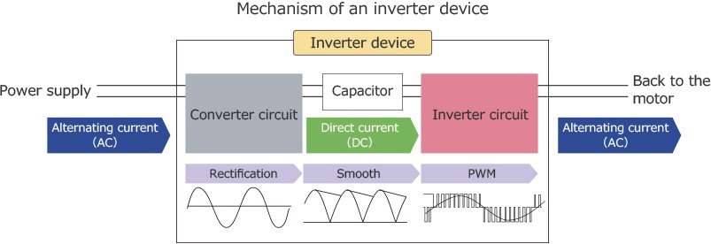
An electrical device or circuit that converts direct current (DC) to alternating current (AC) is known by various terms namely; inverter, power inverter, and invertor [1]. The specific gadget being used determines the final AC frequency. A reverser, which was once a large electromechanical device that converted AC to DC [2], is the inverse of an inverter. The input voltage, resultant voltage, frequency range, and total power management of a device or circuit are determined by its design. The DC source generates electricity, not the converter. A power inverter might consist completely of electrical components, or it can include both electronic circuitry and mechanical components, such as spinning machinery. During the conversion process, static inverters do not use moving components. An analogous purpose is served by circuits referred to as oscillators for electronic signals, which typically have very low voltages and currents. Power inverters are often used in high-current and high-voltage electrical power applications. Conversely, circuits known as rectifiers convert AC to DC.
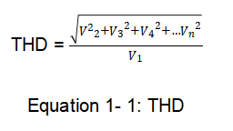
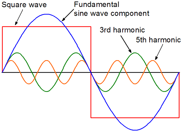
In a simple inverter circuit, DC power is applied to the center tap of a transformer’s primary winding. One end of the main winding is swiftly swapped back and forth, allowing current to go back to the DC source via two distinct paths. When the direction of the current in the main winding changes, an alternating current (AC) is produced in a transformer’s secondary circuit. The switching device’s electromechanical construction consists of one moving contact that is supported by a spring and two fixed contacts. The spring keeps the mobile contact against one of these fixed contacts, but an electromagnet pushes it against the opposite stationary contact. The switch’s action stops the electromagnet’s current, making it continuously flip swiftly back and forth. These electromechanical inverter switches, sometimes referred to as buzzers or vibrators, were first used in vacuum tube automobile radios. Tattoo machines, doorbells, and buzzers have all employed a similar idea. When available with sufficient power ratings, transistors, along with other semiconductor switching devices, have been used in inverter circuit designs. In some ratings, thyristors (SCR) are used, particularly for big systems (kilowatts or more). SCRs are a kind of semiconductor device with a large power handling capability and easy regulation over a wide firing range. The basic inverter’s simple on/off switch allows it to create a square voltage waveform instead of the usual sinusoidal waveform of an AC power source when it’s not linked to an output transformer. Using Fourier analysis, periodic waveforms are represented as the sum of an infinite series of sine waves. The sine wave, which has the exact same frequency as the original waveform, is the fundamental part. The following sine wave frequencies in the series are integral multiples of the fundamental frequency, which are referred to as harmonics.
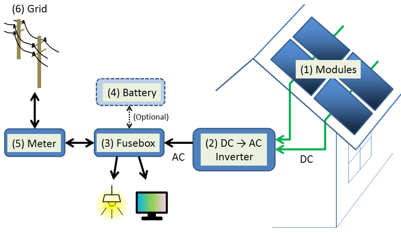
Fourier analysis may be used to calculate the total harmonic distortion (THD). The square of the product of the sum of the square roots of the harmonic voltages divided by the fundamental voltage is how total harmonic distortion, or THD, is computed. This is shown below:
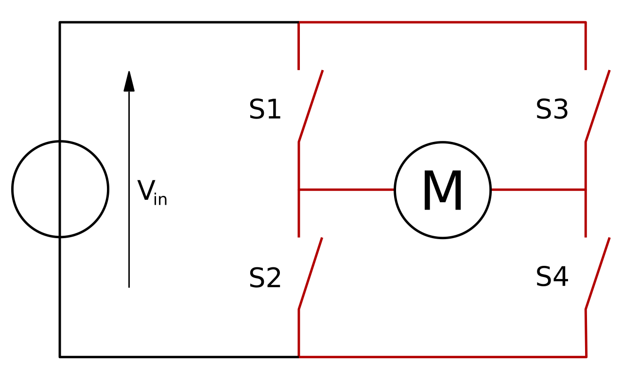
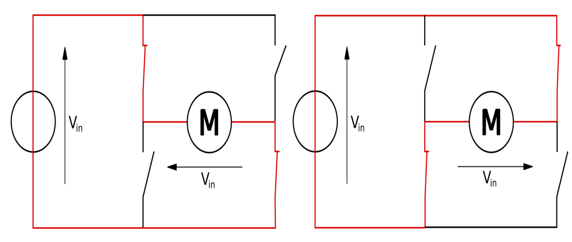
This type of circuit is commonly represented graphically, which is where the word “H-bridge” comes from. An H-bridge is made up of four mechanical or solid-state switches. As shown in the first figure, when switches S1 and S4 are closed and switches S2 and S3 are left open. To reverse this voltage, the motor may open the S1 and S4 switches and shut the S2 and S3 switches. According to the nomenclature above, it is never a good idea to close switches S1 and S2 simultaneously, since this might result in a short circuit on the voltage source for the input. This also holds true for the modifications to S3 and S4. This state is called “shoot-through.”
A two terminal equipment is powered by an H bridge. It is possible to modify the device’s electrical polarities by properly arranging the switches.
1.1 Problem Statement
The current study’s goal is to improve the output waveform quality by creating a multilayer single-phase H-bridge cascade inverter. Nonetheless, there is still a need to provide a thorough technical summary of this research. Inverters are essential in many applications that use renewable energy sources because they ensure that locations with little or no grid connection receive high-quality electricity to fulfill customer demand for electrification. In particular, in photovoltaic systems, the inverter—typically a PWM VSI (Voltage Source Inverter)—converts the DC electrical energy produced by solar modules or arrays into AC voltage suitable for feeding into systems or powering loads. Therefore, it is imperative to address the need for improving the output waveform and voltage levels when using both medium- to high-level and lower-level DC voltage sources.
2. METHODOLOGY
The next procedure is followed in a data-based manner to achieve the project’s goal:
- Carry out a literature review of Electrical power inverter works, Photovoltaic applications and Multilevel inverters
- Design the proposed system using PLECS software
- Run the simulation with system parameters using the PLECS software
3. LITERATUE REVIEW
3.1 Introduction to Photovoltaic Systems
The fluctuating direct current (DC) that exits from a photovoltaic solar panel is converted into the form of an alternating current with a utility-grade frequency (AC) by the solar inverter, also commonly called a photovoltaic, or PV, inverter. Following that, this AC can be used by an industrial electrical grid or a nearby off-grid electrical system. It is a crucial balance of system (BOS) component that permits the use of standard AC-powered solar system equipment. Solar power inverters have features specifically developed for photovoltaic array applications detect maximum power points and prevent islands.
3.1.1 Classification of photovoltaic systems
- The courses are as follows: Stand-alone inverters: they are used in independent power systems and draw DC power from solar-panel-fed batteries. Many standalone inverters also include built-in chargers for batteries to top off the battery when an AC source is available. Since they often don’t interact with the electrical system in any manner, anti-islanding security is not required.
- Grid-tie inverters that use a sine wave provided by the utility to calculate the phase. For safety purposes, grid-tie inverters are made to automatically turn off when the utility’s power is switched off. They don’t provide backup power during power outages.
- Specialized inverters known as battery backup inverters are made to extract power from a power source, control its charge using an integrated charger, and export extra energy straight to the utility grid. These inverters must have certain anti-islanding characteristics and be able to supply certain loads with AC power in the event of a utility interruption.
- Intelligent hybrid inverters are in charge of the solar array, battery storage, utility grid, and direct connection to the unit. Although these contemporary all-in-one systems are sometimes quite adaptable and may be utilized for stand-alone, backup, or grid-tie applications, their main purpose is personal consumption through storage.
3.2 DC to AC inverters
DC-to-AC converters are used to convert a DC source’s waveform into an AC output. Variable-speed drives (VSD), flexible AC transmission systems (FACTS), voltage compensators, uninterruptible power supplies (UPS), and solar inverters are a few examples of applications. There are two basic topologies for these converters: current inverters and voltage inverters. A voltage waveform, or VSI, is the voltage generated by an inverter’s independently regulated output is known as a voltage waveform, or VSI for short. Current source inverters (CSIs) differentiate themselves by using the regulated AC output to create a current waveform. Devices that switch electricity convert DC to AC power. They are often completely programmable power switches made of semiconductors. The output waveforms show abrupt transitions rather than smooth ones since they are composed of discrete integers. Even a crude approximation of the AC power’s sinusoidal waveform suffices for many purposes. When a nearly sinusoidal waveform is required, the switching elements are operated at a rate significantly faster than the desired output frequency, and the duration of time in each state is regulated to create an almost sinusoidal average output. Common modulation techniques include the space-vector technique, the selective-harmonic technique, and the carrier-based approach, commonly referred to as pulse-width modulation [11]. For both single- and three-phase applications, voltage source inverters are useful equipment many high-power, complicated topologies use single-phase virtual switching devices (VSIs) with isolation. These include single-phase UPSs, multicellular electrical arrangements, and half-bridge and full-bridge setups. . Three-phase VSIs are required for applications that require sinusoidal voltage waveforms, such as ASDs, UPSs, and some FACTS devices like the STATCOM. Additionally, they find employment in voltage compensators and active power filters, among other applications where varying voltages are necessary. [11] With current-source inverters, a DC current supply can be converted into an AC output current. This type of inverter makes sense when using three phases and demanding high-quality voltage waveforms.
The multi-level inverter is a relatively new type of inverter that is gaining a lot of attention. When functioning correctly, power switches on CSIs and VSIs are regarded as two-level inverters since they are connected to both the positive and negative DC buses. If the inverter’s output terminals could access more than two voltage levels, the AC output may more nearly approach a sine wave. For this reason, multilayer inverters, despite their higher cost and complexity, offer superior performance [10]. Depending on the kind of inverter, different DC connections may be used, and freewheeling diodes may or may not be required. Both may be set up to operate in square-wave or pulse-width modulation (PWM) mode, depending on how they are utilized. Although PWM may be applied in many ways and produce higher-quality waveforms, square-wave mode is easier to use [11]. An almost constant-voltage source is fed into the output inverter portion using Voltage Source Inverters (VSI) [11]. What is desired from the current output waveform determines which modulation approach is best for a certain application. Discrete values make up a VSI’s output. To provide a uniform current waveform at the chosen harmonic frequencies, the loads must be regarded as inductive in order to provide a uniform current waveform. When a capacitive load is connected without any kind of inductive filtering between the power source and the load, it will exhibit a choppy current waveform with big, frequent current spikes. [11]
There are three main types of VSIs:
- Single-phase half-bridge inverter
- Single-phase full-bridge inverter
- Three-phase voltage source inverter
4. METHODOLOGY
4.1 Research Approach
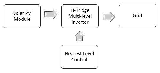
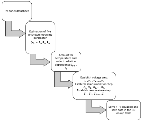
A seven-level cascaded H-bridge multi-level inverter is used in the study to turn the DC output of a solar PV system into an AC wave that takes nonlinear properties into account. The grid to which the system is connected. Figure 4-1 shows the block diagram of the system, which is constructed using PLECS as a model that is dependent on voltage and solar insolation. It shows the solar PV module linked in series (to amplify the DC input voltage as necessary). A 3D look-up table that accounts for current values for various voltage, temperature, and sun irradiation values represents the non-linear features of a photovoltaic module. To convert the PV’s DC output into an AC wave, the multi-level inverter is connected to the PV string. The seven-level cascaded H-bridge is used in this study because of its ability to produce AC waves with little total harmonic distortion. The power semiconductor’s control signal is sent to the inverter using the Nearest Level Control Strategy. When using high-level inverters, a basic approach called closest-level control should be used. When the NLC technique is applied to low-level inverters, it results in lower-order harmonics that are very challenging to remove. The grid receives the inverter’s regulated AC output.
4.2 Modeling the Solar PV
The lookup table may represent any number of series-connected modules by computing the voltage input by dividing the output voltage by the number of modules in the string. Regarding the PV string concept, sunlight is an external component, and voltage is an internal feedback signal. It should be noted that the output capacitance included in the PV string model eliminates the PV current’s dependence on the load current. In this study the PV module used is BP 365, 65W there are 22 PV modules in a string and 2 strings in parallel.
You can download the Project files here: Download files now. (You must be logged in).
To estimate the five parameters of the solar PV circuit, researchers have used a variety of methods. To construct the 3D lookup table on PLEC, the procedure shown in Fig. 4-3 would have to be followed.
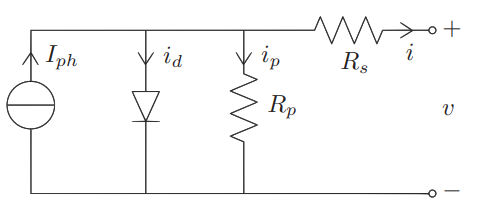
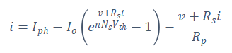
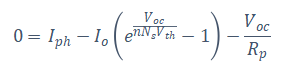
The following formulas use different factors to express the five parameters of the circuit shown in Figure 4-1. The datasheet for the PV module contains the input values for the equation. Equation 4-1’s short circuit current at STC at the short circuit state (, ) yields:
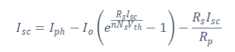
The knowledge that the photo current () is close to zero and the effect of the last term is very small, gives the justification that:
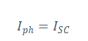
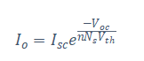
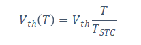
where, from Equation 4-1 at the open circuit state, is the photovoltaic (PV) module open circuit voltage at STC ( ) leads to:
Adopting Equation 4-4 and considering that as well as , the relation holds that:
The temperature factors obtained from the datasheet may be used to calculate the diode ideality factor equation. This is the diode-ideality ratio expression:
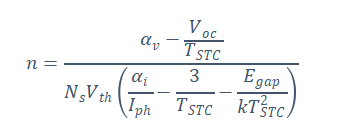
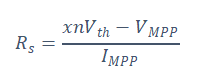
Where is the short circuit voltage temperature coefficient in , is the silicon band gap energy, is the open circuit voltage temperature . The series and parallel resistance are given in Equations 4-8 and 4-9, in which are the Maximum point current and voltage respectively
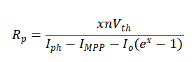
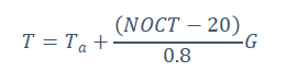
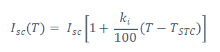
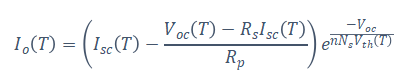
It is necessary to consider the parameters’ dependence on temperature and sun irradiation in order to create a model that can be used for any value of these environmental factors. It shall be assumed that the only two parameters that are dependent on temperature and exposure to sunlight are the diode dark saturation current as well as the photo-current I_{ph}(G, T) and I_o(T) respectively. In order to get an expression for I_o(T), the temperature dependence on short circuit is shown below:
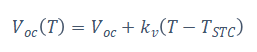
Thus, the temperature dependence of the thermal voltage and the open circuit voltage is given as follows:
Which gives the resulting relation for Io (T) :
Also, the relation for is shown below:
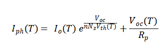
Finally, the relationship between the photocurrent, temperature, and sun irradiation is:
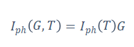
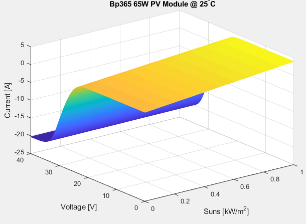
When the impact of environmental conditions that differ from STC is considered, the five relevant criteria become: , , , and . Together, the aforementioned parameters provide a 3D lookup table that can be used in PLECS and mimics the PV model. The current surface data is recorded in an a.mat file and includes information for the usual V-I curves for voltage levels between 0 and 25 V, as shown in Figure 4-4.
The current surface data is recorded in an a.mat file, as shown in Figure 4-4, and includes information for the usual V-I curves for voltages that range between 0 and 25 V and insolation values between 0 and 1 kWhr/m^2, and three distinct temperatures of 0°C, 25°C, and 50°C.
4.3 Multilevel Inverter Topology
A seven-level hybrid cascaded H-bridge multilevel inverter has two H-bridges for each phase, one connected to a DC source and the other to a capacitor. This is shown in Figure 1. For the second H-bridge (H_2), a capacitor voltage fixed at V c would serve as the DC source, and for the first H-bridge (H_1), a power source like a battery or fuel cells with an output voltage of V dc. The cascaded multilevel inverter’s output voltage is as follows:
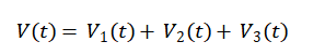
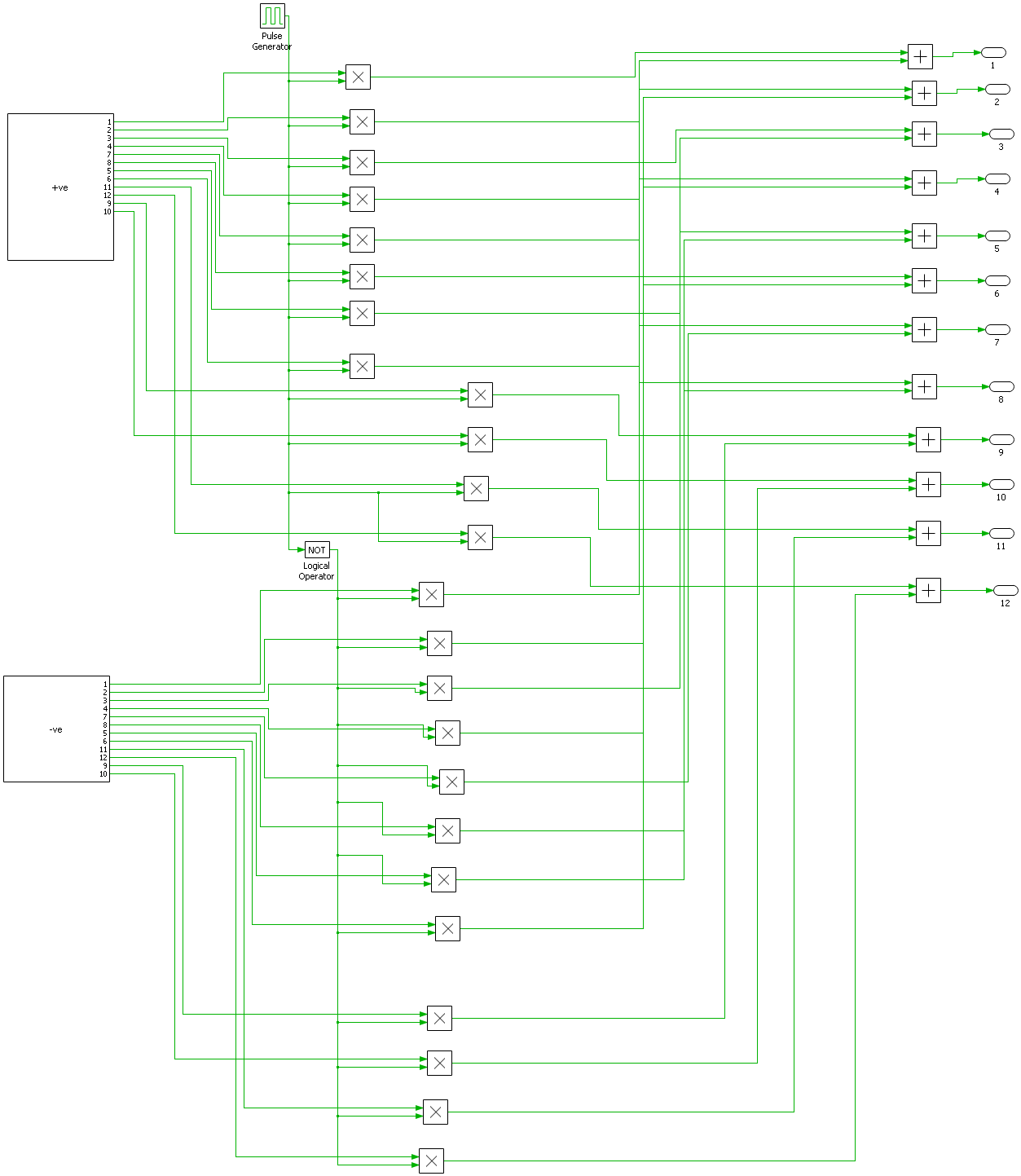
Switches on and off on allow the output voltage V_1 to be adjusted to , 0, or , while ‘s switches can be turned on and off to set the output voltage to , 0, or . And for the ’s the output voltage to be adjusted to , 0, or . Figures 4-5 and Table 4-1, respectively, display the structure of the switching table and the 7-level cascaded H-bridge inverter.
| Levels | V | ||||||||||||
| 1 | 1 | 0 | 0 | 1 | 1 | 0 | 0 | 1 | 1 | 0 | 0 | 1 | |
| 2 | 0 | 1 | 1 | 0 | 1 | 0 | 0 | 1 | 1 | 0 | 0 | 1 | |
| 3 | 0 | 1 | 0 | 1 | 1 | 0 | 0 | 1 | 1 | 0 | 0 | 1 | |
| 4 | 0 | 0 | 0 | 0 | 0 | 0 | 0 | 0 | 0 | 0 | 0 | 0 | 0 |
| 5 | 1 | 0 | 0 | 1 | 0 | 1 | 1 | 0 | 0 | 1 | 1 | 0 | |
| 6 | 0 | 1 | 1 | 0 | 0 | 1 | 1 | 0 | 0 | 1 | 1 | 0 | |
| 7 | 0 | 1 | 0 | 1 | 0 | 1 | 1 | 0 | 0 | 1 | 1 | 0 |
Table 4 -. 1: Switching Pattern for Cascaded H-Bridge with Unequal Voltage Sources—Seven Level
4.4 Nearest Level Modulation Control Strategy
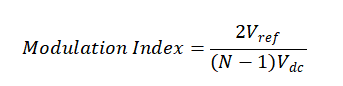
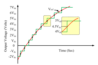
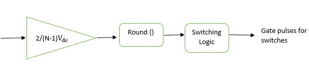
In high-voltage applications, two types of closest-level control techniques are employed: nearest space vector control and nearest-level control approaches. By employing the closest control approaches, lower-order harmonics are eliminated, and switching losses are decreased. The NLC technique runs at 50 or 60 Hz and can be extended to the N level. The study used nonlinear control (NLC) to control the output voltage of the proposed fundamental unit of the multi-level inverter. Figures 4-6 and 4-7 show the NLC approach. Modifications to the NLC’s V_ref can alter the modulation index (MI), which has the following definition:
You can download the Project files here: Download files now. (You must be logged in).
The control diagram makes it evident how the value’s gain block is applied to the reference signal V ref (sinusoidal). . The round function is given the ratio / , This establishes the closest voltage level that the inverter uses to generate its switching logic and switch gating signals. The synthesized waveform shows that the initial voltage cuts exactly at the staircase waveform’s halfway point when the round0.5 {} function is used. The table below depict the simulation parameters in the study. The figures 4-9, 4-10, 4-11, 4-12 illustrate the plant simulation schematic, nearest level control first level simulation schematic, nearest level control second level simulation schematic, nearest level control second level 1 level simulation schematic.
| Parameter | Value |
| Grid voltage | 230V |
| Grid frequency | 50Hz |
| 1mH | |
| 0.2mH | |
| 5µF | |
| PV Power | 3kW |
| No. PV module in String | 22 |
| No. PV module in Parallel | 2 |
Table 4 – 2: Simulation Parameters
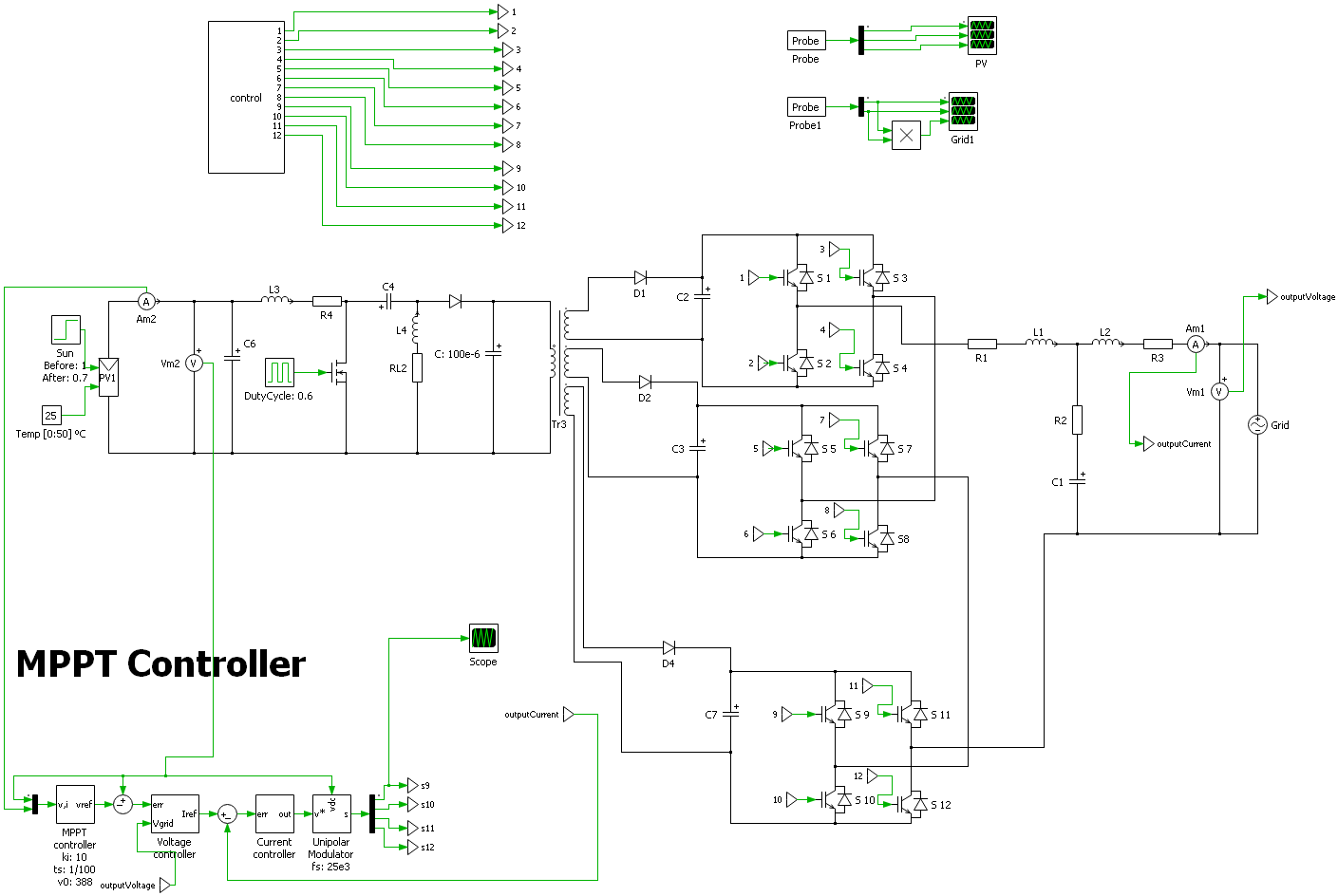
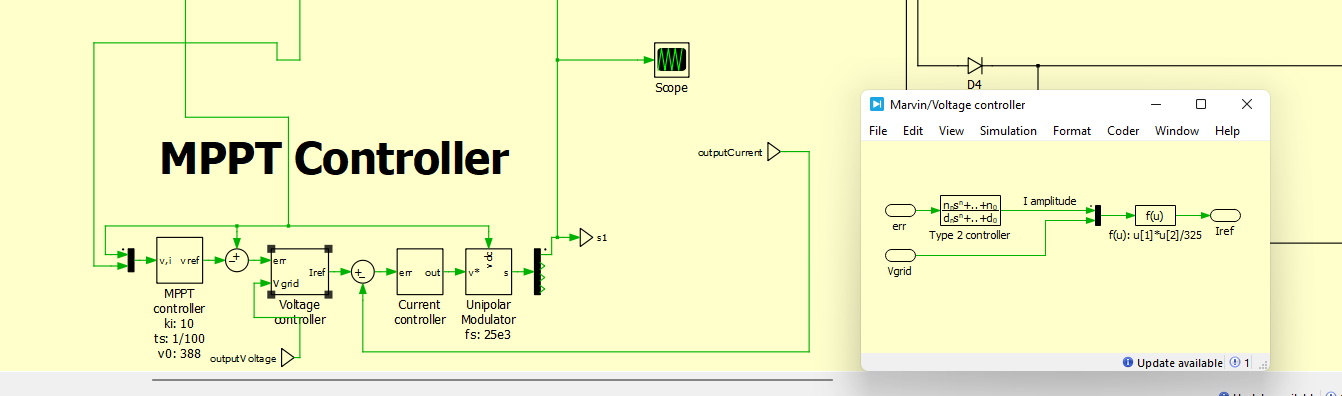
The simulation scheme for a PV system combined with an open loop MPPT (Maximum Power Point Tracking) controller is shown in Figure 4-12. The relationship between the grid, the MPPT controller, and the PV array is shown in this graphic. The MPPT controller then optimizes the electrical power produced by the PV array to guarantee that the maximum amount of power is extracted from the PV modules. To keep the PV array producing the most power possible, the controller modifies the array’s operating point. The schematic also contains an inverter for converting DC electricity from the PV array into AC power suitable for grid connection. Additionally, numerous sensors and feedback loops are built to monitor and control voltage, current, and power parameters, assuring efficient and steady operation of the system.
5. RESULTS
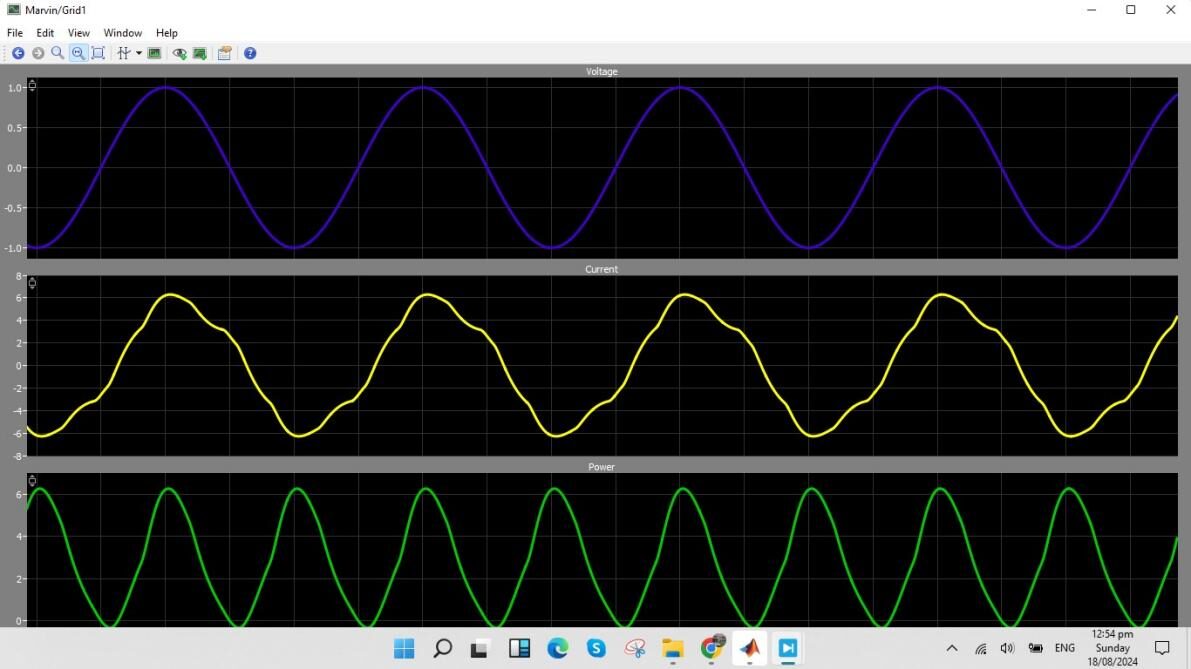
The cascaded H-bridge seven-level inverter simulation with a grid-connected photovoltaic module’s output demonstrates the feasibility of using solar energy for grid integration. The transfer of power from the PV module to the grid is expressed as shown in Figure 5-1, which clearly illustrates the energy supply. The power factor is calculated to be 0.4687. Additionally, sinusoidal waveforms that are in phase with the grid’s voltage and current are seen, indicating the stability of operating in tandem with the grid. The inverters’ capacity to filter the waveform effectively ensures grid stability and high-quality power, as seen by the grid voltage’s lack of harmonics. The study’s results show that the seven-level cascaded H-bridge seven-level inverter works well and reliably in grid-connected photovoltaic applications. They also show that it has the potential for clean energy generation and grid-tied applications while keeping power quality and stability.
You can download the Project files here: Download files now. (You must be logged in).
A PV module’s output power waveform typically consists of pulses, the strength of which varies according to the amount of sunshine present. The behavior is designed so that power production is high at solar maximums and low during solar minimums. Sunlight availability also affects the PV module’s voltage and current waveforms. The PV module’s output voltage and current are highest when sunshine is at its strongest; when sunlight is scarce, the output waveform battery voltage and current are lower. This essentially demonstrates that the PV module’s voltage, current, and power are all closely correlated with the incident solar radiation. The PV module’s output power, voltage, and current waveforms are displayed in Figure 5-2.
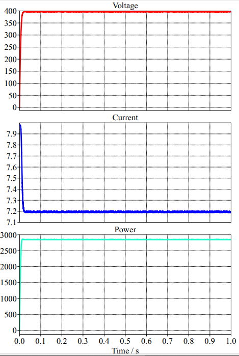
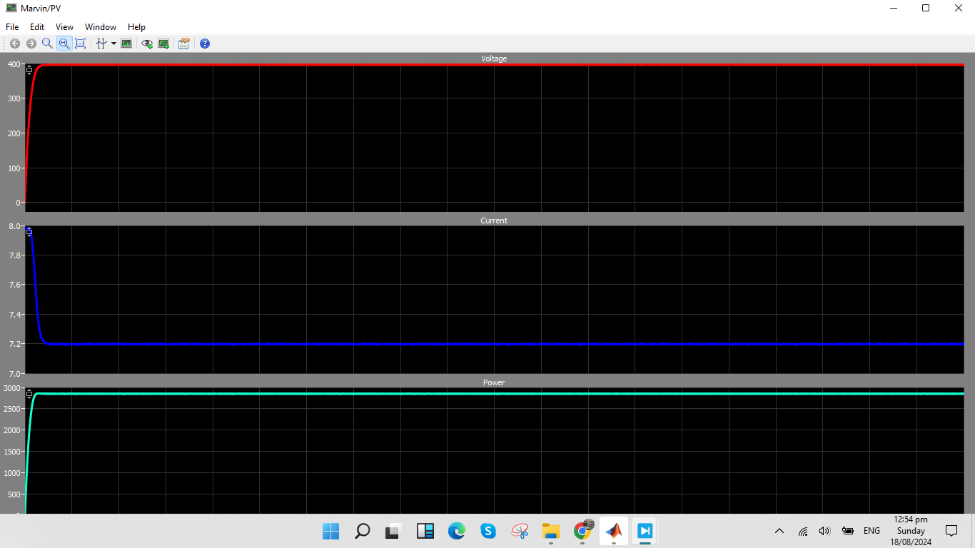
The PV module’s voltage, current, and power output waveforms when connected to the grid are shown in Figure 5-3. The MPPT controller maintains a constant DC voltage level in the voltage waveform to maximize power output. The PV module’s generated current, which is contingent upon temperature and solar irradiation, is represented by the current waveform. The PV module’s immediate power delivery is shown by the power output waveform, which is a function of both voltage and current. These waveforms demonstrate how well the MPPT controller maintains optimal performance in spite of variations in the external environment since the power output stays constant. The graph effectively illustrates the PV system’s dynamic responsiveness to variations in solar input, guaranteeing optimal energy extraction.
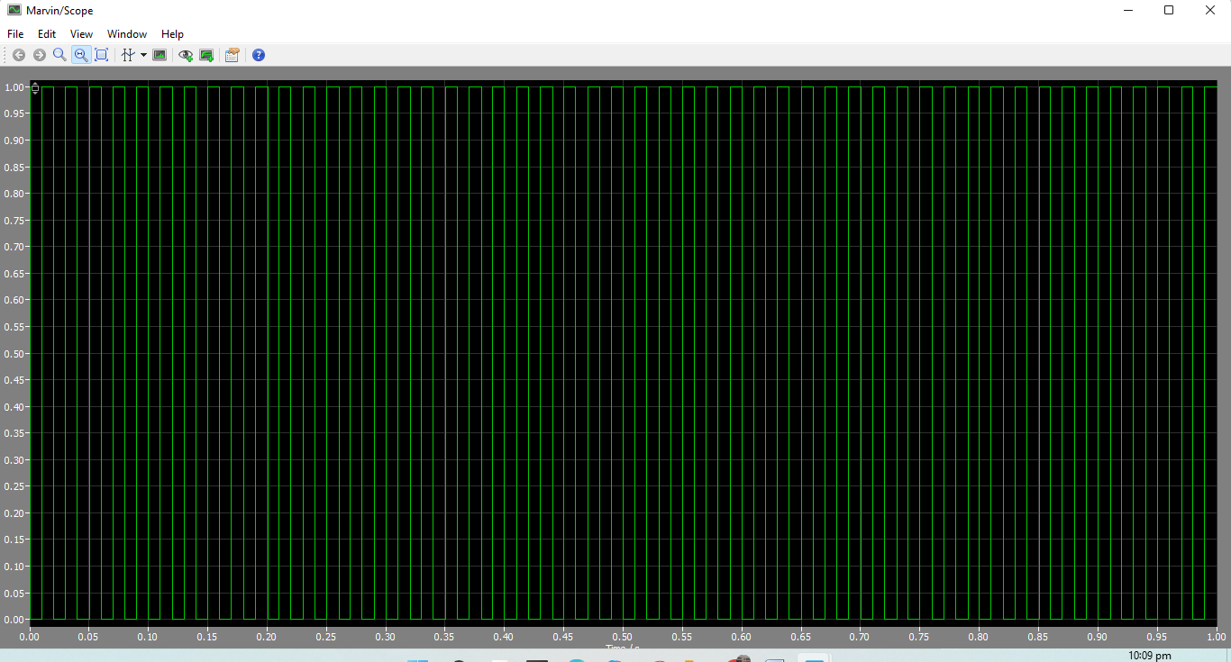
The PV module’s Pulse Width Modulation (PWM) output waveform with MPPT control when connected to the grid is shown in Figure 5-4. To make sure the PV module runs at its maximum power point, the PWM signal is employed to control the power converter. The waveform displays a sequence of high-frequency pulses with variable duty cycles that dynamically align with the PV module’s ideal operating point. Precise control over the power converter is made possible by the modulation of the PWM signal’s duty cycle, which is dependent on feedback from the PV module’s voltage and current outputs. The entire efficiency of the solar energy system is increased by this modulation, which guarantees that the PV module continuously supplies the grid with its maximum output. Features of the waveform, including changes in frequency and duty cycle, are a reflection of the constant modifications the MPPT controller makes to react to the sun’s shifting conditions.
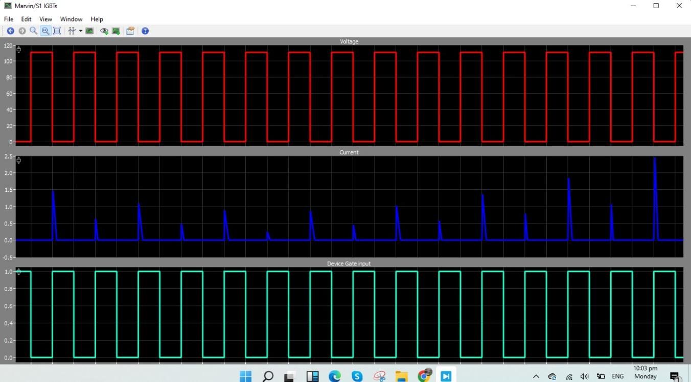
Insulated gate bipolar transistors (IGBTs) in an H-bridge circuit are shown with their gate input and output waveforms in Figure 5-5, which also shows the voltage and current characteristics during operation. The control signals applied to the IGBT gates—typically in the form of PWM signals—which determine how the transistors switch are displayed in the gate input waveform. The discrete on and off states of these signals regulate the IGBTs’ conduction durations, guaranteeing the H-bridge operates well.
The voltage waveform at the H-bridge’s output shows the AC voltage that results from the IGBTs’ switching operation. The bidirectional current flow that is necessary to drive AC loads is reflected in this waveform’s typical alternating positive and negative values. The H-bridge’s function in transforming a DC input into a regulated AC output is demonstrated by the abrupt changes in the waveform, which match to the exact switching instants identified by the gate input signals.
The current passing through the load attached to the H-bridge is shown by the current waveform. The parameters of the load and the IGBTs’ switching frequency have an impact on the waveform’s shape. The IGBT switching causes the current to increase during on times and drop during off times. The H-bridge circuit operates at its best with little loss thanks to the efficient management of current flow.
Together, these waveforms show how important IGBT gate control is for controlling the voltage and current in the H-bridge, allowing for effective power conversion and regulation for a range of uses. Accurate control is essential in power electronic circuits because the desired performance depends on the precise timing and modulation of the gate input signals.
The table below shows the analysis of the grid THD which are ascertained from the PLECS scope cursor feature.
| Result | Value |
| Total Harmonic Distortion | , |
6. CONCLUSION AND FURTHER STUDIES
For photovoltaic modules that are connected to the grid, using the closest level modulation control along with cascaded seven-level H-bridges has a number of benefits. The closest level control, which reduces switch switching losses in the MLI topology and ensures higher-quality power is sent into the grid, significantly improves the system’s performance. Compared to alternative modulation approaches like selective harmonic removal, the simulation signals used in this study’s control methodology can improve switching efficiency, reduce harmonic distortion, and produce superior power quality. As a result, grid-connected PV systems can benefit from using the cascaded seven-level H-bridge with the closest level modulation control.
It would be helpful to do more research in a number of areas about how to use nearest level modulation control and cascaded seven-level H-bridges for photovoltaic systems that are connected to the grid. A few of these potential study areas are listed below;
- The advancement of more effective modulation methods that may further enhance the grid’s power injection quality and guarantee a better supply for consumers who are connected. Moreover, the control method should be optimized to offer reliable performance under varied circumstances.
- Research on enhancing the adaptability of smart grids by the incorporation of the suggested method to guarantee increased flexibility and dependability of the smart grid.
- Moreover, validation of the experimental data may be carried out to confirm the conclusion drawn from the suggested system, providing a clear illustration of the suggested approach’s capacity to perform its intended function.
To put it simply, research into these areas can help electrify rural areas and other non-grid locations, as well as improve the efficiency and performance of grid-connected photovoltaic systems in the future to satisfy the growing demand for high-quality supplies worldwide.
REFERENCES
[1] The Authoritative Dictionary of IEEE Standards Terms, Seventh Edition, IEEE Press, 2000,ISBN 0-7381-2601-2
[2] “Inverter frequently asked questions”. Powerstream.com. Retrieved 2020-11-13
[3] https://commons.wikimedia.org/w/index.php?curid=4845234
[4] https://commons.wikimedia.org/w/index.php?curid=52772789
[5] Williams, A. (2002, January 3). Microcontroller Projects Using the Basic Stamp. https://doi.org/10.1201/9781482 280777
[6] Unruh, R., Schafmeister, F., & Bocker, J. (2020, November 9). 11kW, 70kHz LLC Converter Design with Adaptive Input Voltage for 98% Efficiency in an MMC. 2020 IEEE 21st Workshop on Control and Modeling for Power Electronics (COMPEL)
[7] https://commons.wikimedia.org/w/index.php?curid=854051
[8] https://commons.wikimedia.org/w/index.php?curid=854125
[9] https://commons.wikimedia.org/w/index.php?curid=17181966
[10] Trzynadlowski, A. M. (2015, October 19). Introduction to Modern Power Electronics. John Wiley & Sons.
[11] Rashid, M. H. (2010, July 19). Power Electronics Handbook
[12] Kiruthiga, M. R. S. (2017). Modern Physics, 18th Edition. S. Chand Publishing
[13] https://en.wikipedia.org/w/index.php?curid=35216949
[14] https://en.wikipedia.org/w/index.php?curid=35216995
[15] https://en.wikipedia.org/w/index.php?curid=35218498
[16] https://en.wikipedia.org/w/index.php?curid=35218568
[17] https://en.wikipedia.org/w/index.php?curid=35218760
[18] Single-phase full-bridge inverter with multiple pulse width modulation. (2017, May 6). Physics Forums: Science Discussion, Homework Help, Articles
[19] https://en.wikipedia.org/w/index.php?curid=35219029
[20] https://en.wikipedia.org/w/index.php?curid=35219123
[21] https://en.wikipedia.org/w/index.php?curid=35218760
[22] Balal, A., Dinkhah, S., Shahabi, F., Herrera, M., & Chuang, Y. L. (2022, February 1). A Review on Multilevel Inverter Topologies. Emerging Science Journal, 6(1), 185–200.
[23] Keddar, M., Doumbia, M. L., Krachai, M. Della, Belmokhtar, K., & Midoun, A. H. (2019). Interconnection performance analysis of single phase neural network based NPC and CHB multilevel inverters for grid-connected PV systems. International Journal of Renewable Energy Research, 9(3), 1451–1461
[24] Nguyen, N. V., Nguyen, T. K. T., & Lee, H. H. (2014). A reduced switching loss PWM strategy to eliminate common-mode voltage in multilevel inverters. IEEE Transactions on Power Electronics, 30(10), 5425-5438. https://doi.org/10.1109/TPEL.2014.2377152
[25] Chowdhury, M. R., Rahman, M. A., Islam, M. R., & Mahfuz-Ur-Rahman, A. M. (2021). A New Modulation Technique to Improve the Power Loss Division Performance of the Multilevel Inverters. IEEE Transactions on Industrial Electronics, 68(8), 6828–6839. doi:10.1109/TIE.2020.3001846.
[26] Hossam-Eldin, A. A., Negm, E., Elgamal, M. S., & AboRas, K. M. (2020). Operation of grid-connected DFIG using SPWM- and THIPWM-based diode-clamped multilevel inverters. IET Generation, Transmission and Distribution, 14(8), 1412–1419. doi:10.1049/iet-gtd.2019.0248
[27] Wu, B. and M. Narimani, (2016). Diode-Clamped Multilevel Inverters in High-Power Converters and AC Drives, 143–183. doi:10.1002/9781119156079.ch8
[28] Choudhury, S., Nayak, S., Dash, T. P., & Rout, P. K. (2018). A comparative analysis of five level diode clamped and cascaded H-bridge multilevel inverter for harmonics reduction. In International Conference on Technologies for Smart City Energy Security and Power: Smart Solutions for Smart Cities, ICSESP 2018 – Proceedings (Vols. 2018-January), 1–6. IEEE. doi:10.1109/ICSESP.2018.8376690
[29] Narendra Rao, P., & Nakka, J. (2019). A Novel Hybrid Multilevel PWM Technique for Power Rating Enhancement in Improved Hybrid Cascaded Diode Clamped Multilevel Inverter. Electric Power Components and Systems, 47(11–12), 1132–1143. doi:10.1080/15325008.2019.1659455
[30] Shi, S., Wang, X., Zheng, S., Zhang, Y., & Lu, D. (2018). A new diode-clamped multilevel inverter with balance voltages of DC capacitors. IEEE Transactions on Energy Conversion, 33(4), 2220–2228. doi:10.1109/TEC.2018.2863561
[31] Hassan, P. D. R., & Shyaa, S. S. (2021). Simulink Implementation of Voltage Stability Improvements Using STATCOM based 5-level Diode Clamped Converter. IOP Conference Series: Materials Science and Engineering, 1105(1), 012009. doi:10.1088/1757-899x/1105/1/012009
[32] Adam, G. P., Finney, S. J., Massoud, A. M., & Williams, B. W. (2008). Capacitor balance issues of the diode-clamped multilevel inverter operated in a quasi-two-state mode. IEEE Transactions on Industrial Electronics, 55(8), 3088–3099. doi:10.1109/TIE.2008.922607
[33] Von Bloh, J., & De Doncker, R. W. (2002). Design rules for diode-clamped multilevel inverters used in medium-voltage applications. International Power Electronics Congress – CIEP, 2002-January, 165–170. doi:10.1109/CIEP.2002.1216654
[34] Escalante, M. F., Vannier, J. C., & Arzandé, A. (2002). Flying capacitor multilevel inverters and DTC motor drive applications. IEEE Transactions on Industrial Electronics, 49(4), 809–815. doi:10.1109/TIE.2002.801231
[35] Humayun, M., Khan, M. M., Hassan, M. U., & Zhang, W. (2021). Analysis of hybrid switches symmetric flying capacitor multilevel inverter based STATCOM. International Journal of Electrical Power and Energy Systems, 131, 107054. doi:10.1016/j.ijepes.2021.107054
[36] Coday, S., Barchowsky, A., & Pilawa-Podgurski, R. C. N. (2021). A 10-level gan-based flying capacitor multilevel boost converter for radiation-hardened operation in space applications. Conference Proceedings – IEEE Applied Power Electronics Conference and Exposition – APEC, 2798–2803. doi:10.1109/APEC42165.2021.9487143
[37] Humayun, M., Khan, M. M., Muhammad, A., Xu, J., & Zhang, W. (2020). Evaluation of symmetric flying capacitor multilevel inverter for grid-connected application. International Journal of Electrical Power and Energy Systems, 115, 105430. doi:10.1016/j.ijepes.2019.105430
[38] Barth, C. B., Assem, P., Foulkes, T., Chung, W. H., Modeer, T., Lei, Y., & Pilawa-Podgurski, R. C. (2019). Design and control of a GaN-based, 13-level, flying capacitor multilevel inverter. IEEE Journal of Emerging and Selected Topics in Power Electronics, 8(3), 2179-2191. https://doi.org/10.1109/JESTPE.2019.2956166
[39] Abhilash, T., Annamalai, K., & Tirumala, S. V. (2019). A Seven-Level VSI with a Front-End Cascaded Three-Level Inverter and Flying-Capacitor-Fed H-Bridge. IEEE Transactions on Industry Applications, 55(6), 6073–6088. doi:10.1109/TIA.2019.2933378
[40] Amini, J., & Moallem, M. (2017). A Fault-Diagnosis and Fault-Tolerant Control Scheme for Flying Capacitor Multilevel Inverters. IEEE Transactions on Industrial Electronics, 64(3), 1818–1826. doi:10.1109/TIE.2016.2624722
[41] Porselvi, T., & Muthu, R. (2011). Comparison of cascaded H-bridge, neutral point clamped and flying capacitor multilevel inverters using multicarrier PWM. Proceedings – 2011 Annual IEEE India Conference: Engineering Sustainable Solutions, INDICON-2011. doi:10.1109/INDCON.2011.6139534
[42] Adam, G. P., Anaya-Lara, O., Burt, G., Finney, S. J., & Williams, B. W. (2009). Comparison between flying capacitor and modular multilevel inverters. IECON Proceedings (Industrial Electronics Conference), 271–276. doi:10.1109/IECON.2009.5414934
[43] Wu, B., & Narimani, M. (2017). Cascaded H‐bridge multilevel inverters
[44] Chithra, M., & Dasan, S. G. B. (2011). Analysis of cascaded H bridge multilevel inverters with photovoltaic arrays. 2011 International Conference on Emerging Trends in Electrical and Computer Technology, ICETECT 2011, 442–447. doi:10.1109/ICETECT.2011.5760157
[45] Odeh, C. I., Lewicki, A., & Morawiec, M. (2021). A Single-Carrier-Based Pulse-Width Modulation Template for Cascaded HBridge Multilevel Inverters. IEEE Access, 9, 42182–42191. doi:10.1109/ACCESS.2021.3065743
[46] Memon, M. A., Siddique, M. D., Saad, M., & Mubin, M. (2021). Asynchronous Particle Swarm Optimization-Genetic Algorithm (APSO-GA) based Selective Harmonic Elimination in a Cascaded H-Bridge Multilevel Inverter. IEEE Transactions on Industrial Electronics. doi:10.1109/TIE.2021.3060645
[47] Lee, E. J., Kim, S. M., & Lee, K. B. (2020). Modified phase-shifted PWM scheme for reliability improvement in cascaded Hbridge multilevel inverters. IEEE Access, 8, 78130–78139. doi:10.1109/ACCESS.2020.2989694
[48] Maurya, S., Mishra, D., Singh, K., Mishra, A. K., & Pandey, Y. (2019). An Efficient Technique to reduce Total Harmonics Distortion in Cascaded H- Bridge Multilevel Inverter. Proceedings of 2019 3rd IEEE International Conference on Electrical, Computer and Communication Technologies, ICECCT 2019. doi:10.1109/ICECCT.2019.8869424
[49] Bhatnagar, P., Agrawal, R., & Gupta, K. K. (2019). Reduced device count version of single-stage switched-capacitor module for cascaded multilevel inverters. IET Power Electronics, 12(5), 1079–1086. doi:10.1049/iet-pel.2018.6017
[50] Khoucha, F., Ales, A., Khoudiri, A., Marouani, K., Benbouzid, M. E. H., & Kheloui, A. (2010). A 7-level single DC source cascaded H-bridge multilevel inverters control using hybrid modulation. 19th International Conference on Electrical Machines, ICEM 2010. doi:10.1109/ICELMACH.2010.5608179
[51] Lee, E. J., & Lee, K. B. (2021). Performance improvement of cascaded H-bridge multilevel inverters with modified modulation scheme. Journal of Power Electronics, 21(3), 541–552. doi:10.1007/s43236-020-00200-w
[52] Tackie, S. N., & Babaei, E. (2020). Modified topology for three-phase multilevel inverters based on a developed H-bridge inverter. Electronics, 9(11), 1848. https://doi.org/10.3390/electronics9111848
[53] Grigoletto, F. B. (2020). Five-Level Transformerless Inverter for Single-Phase Solar Photovoltaic Applications. IEEE Journal of Emerging and Selected Topics in Power Electronics, 8(4), 3411–3422. doi:10.1109/JESTPE.2019.2891937
[54] Hsieh, C. H., Liang, T. J., Chen, S. M., & Tsai, S. W. (2016). Design and Implementation of a Novel Multilevel DC-AC Inverter. IEEE Transactions on Industry Applications, 52(3), 2436–2443. doi:10.1109/TIA.2016.2527622
[55] Kadam, A., & Shukla, A. (2017). A Multilevel Transformerless Inverter Employing Ground Connection between PV Negative Terminal and Grid Neutral Point. IEEE Transactions on Industrial Electronics, 64(11), 8897–8907. doi:10.1109/TIE.2017.2696460
[56] Siddique, M. D., Mekhilef, S., Mekhilef, S., Shah, N. M., Ali, J. S. M., & Blaabjerg, F. (2020). A new switched capacitor 7L inverter with triple voltage gain and low voltage stress. IEEE Transactions on Circuits and Systems II: Express Briefs, 67(7), 1294–1298. doi:10.1109/TCSII.2019.2932480
[57] Mondol, M. H., Tür, M. R., Biswas, S. P., Hosain, M. K., Shuvo, S., & Hossain, E. (2020). Compact Three Phase Multilevel Inverter for Low and Medium Power Photovoltaic Systems. IEEE Access, 8, 60824–60837. doi:10.1109/ACCESS.2020.2983131
[58] Malinowski, M., Gopakumar, K., Rodriguez, J., & Perez, M. A. (2009). A survey on cascaded multilevel inverters. IEEE Transactions on Industrial Electronics, 57(7), 2197–2206. doi:10.1109/TIE.2009.2030767
[59] Ali, A. N., Jeyabharath, R., & Udayakumar, M. D. (2016). Cascaded Multilevel Inverters for Reduce Harmonic Distortions in Solar PV Applications. Asian Journal of Research in Social Sciences and Humanities, 6(11), 703. doi:10.5958/22497315.2016.01223.5
[60] Kjaer, S. B., Pedersen, J. K., & Blaabjerg, F. (2005). A review of single-phase grid-connected inverters for photovoltaic modules. IEEE Transactions on Industry Applications, 41(5), 1292–1306. doi:10.1109/TIA.2005.853371
[61] N. Mukundan C.M., K. Vineeth, S. S. Kumar and P. Jayaprakash, “Improved H-bridge Multilevel Inverter for Grid Integration of Photovoltaic Power Conversion System with Power Quality Enhancement,” 2020 IEEE International Conference on Power Electronics, Smart Grid and Renewable Energy (PESGRE2020), Cochin, India, 2020, pp. 1-6, doi: 10.1109/PESGRE45664.2020.9070295
[62] A.E.W.H. Kahlane, L. Hassaine and M. Kherchi “LCL filter design for photovoltaic grid connected systems” 2014 Revue des Energies Renouvelables SIENR’14, Ghardaïa, (2014) pp.227 – 232
[63] Electrical Equipment 2024 Centre Tapped Transformer [Online] Available: http://engineering.electrical-equipment.org/electrical-distribution/centre-tapped-transformer.html
You can download the Project files here: Download files now. (You must be logged in).


Responses