

Analysis of Coupling Coefficients in Silicon Photonics Using Analytic and 3D FDTD Methods in MATLAB and Ansys Lumarical
Author: Waqas Javaid
Abstract
This report investigates the coupling coefficients of a 3D silicon photonics structure using both analytical methods and finite-difference time-domain (FDTD) simulations. The primary focus is on a 700 nm x 250 nm strip waveguide operating at a wavelength of 940 nm, with a bending radius of 50 µm. Simulations are conducted using Ansys Lumerical varFDTD, and analytical results are computed using MATLAB. A detailed comparison is presented between the analytic and FDTD results, with insights into the strengths and limitations of each approach. This study contributes to the optimization of silicon photonic circuits for compact and efficient optical signal transmission.
1. Introduction
Silicon photonics has emerged as a transformative platform for implementing high-speed, low-power, and cost-effective photonic integrated circuits (PICs). It leverages the mature CMOS fabrication technology to produce miniaturized photonic components for data communication, sensing, and optical signal processing. Among the key components of a silicon photonic circuit are waveguides, which confine and guide light with high precision. Coupling between waveguides is a fundamental mechanism that governs the operation of various photonic devices, including directional couplers, ring resonators, Mach-Zehnder interferometers (MZIs), and wavelength filters. The coupling behavior is determined by the electromagnetic field overlap between adjacent waveguides, which is influenced by geometrical and material parameters such as waveguide width, height, separation gap, curvature, and refractive index contrast. Understanding and accurately modeling this coupling phenomenon is essential for designing compact and efficient integrated photonic systems [1] [2].
Traditionally, the coupling coefficient between waveguides is derived using analytical approaches based on coupled-mode theory (CMT), which simplifies the problem into manageable mathematical expressions. CMT assumes weak coupling and uniform modes, making it suitable for quick estimations and conceptual understanding. These models provide direct relationships between geometry and optical behavior, offering a fast and insightful tool during the early design phase. However, CMT has limitations in accurately capturing complex 3D interactions, especially in structures with tight bends, high index contrast, or strong coupling [3]. This is where numerical methods such as the finite-difference time-domain (FDTD) technique become invaluable. FDTD methods solve Maxwell’s equations directly in the time domain across discretized 3D structures, enabling detailed visualization of field propagation and mode interaction in realistic geometries.
In this report, we analyze the coupling coefficients of a 700 nm × 250 nm silicon strip waveguide at a 940 nm wavelength using both analytical models and 3D FDTD simulations. The waveguide design includes a curvature radius of 50 µm to simulate realistic device behavior. MATLAB is used to compute the analytical coupling coefficients based on mode overlap integrals, while Ansys Lumerical’s varFDTD tool provides full-wave numerical simulations. A comparative analysis is presented to evaluate the consistency, accuracy, and limitations of both methods. This dual-method approach not only validates the simulation results but also informs future design choices for photonic devices where precision and compactness are critical. Through this study, we aim to bridge the gap between theory and simulation and highlight the practical benefits of using both methods in silicon photonics design workflows.
2. Design Methodology
2.1 Waveguide Geometry and Parameters
The waveguide under investigation is a rectangular silicon strip waveguide with dimensions 700 nm (width) × 250 nm (height). The cladding is silicon dioxide (SiO2), and the core is silicon. The operating wavelength is 940 nm, which is compatible with common photonic applications and corresponds to near-infrared operation [4]. A bending radius of R = 50 µm is chosen to simulate practical conditions in curved waveguides such as microring resonators.
2.2 Analytical Coupling Coefficient Calculation
The coupling coefficient κ in coupled-mode theory is derived based on the overlap integral of the electromagnetic fields in adjacent waveguides:
κ = (ωε₀ / 4) ∫ (Δε) E₁* ⋅ E₂ dA
Here, Δε represents the difference in permittivity between the waveguides, and E₁, E₂ are the electric fields of the two waveguides. The effective indices and mode profiles are computed in MATLAB using eigenmode analysis [5]. This allows rapid estimation of coupling strength as a function of gap and waveguide curvature.
2.3 FDTD Simulation Using Ansys Lumerical
To obtain a more accurate picture of mode interaction, full 3D FDTD simulations are carried out in Ansys Lumerical using varFDTD solver. The structure includes two parallel curved waveguides with a separation gap ranging from 200 nm to 400 nm. The input source is a fundamental TE mode at 940 nm. Perfectly matched layer (PML) boundary conditions are applied.
The coupling coefficient is extracted by monitoring the transmitted power in the through and cross ports, and fitting the results to standard coupled-mode transmission equations [6].
2.4 Comparison Approach
To compare the analytic and FDTD results, the coupling coefficients are normalized and plotted against waveguide separation. Metrics such as coupling length and beat length are also evaluated.
3. Results and Simulations
3.1 Analytical Results
The MATLAB simulation results reveal that the coupling coefficient decreases exponentially with increasing separation between waveguides. For a gap of 200 nm, κ ≈ 0.38 mm⁻¹, whereas at 400 nm, κ ≈ 0.06 mm⁻¹. The coupling length Lc, defined as π / (2κ), ranges from ~4.13 mm (200 nm gap) to ~26.2 mm (400 nm gap).
3.2 FDTD Results
FDTD simulation results confirm the trend observed in analytical calculations. However, the coupling coefficients are slightly lower due to 3D effects and scattering losses. At 200 nm separation, the FDTD-estimated κ ≈ 0.35 mm⁻¹, and at 400 nm, κ ≈ 0.05 mm⁻¹. The field profiles extracted from Lumerical show strong overlap for closer gaps, and weaker interaction as the separation increases. This validates the assumptions used in coupled-mode theory but also highlights limitations of 2D approximations in analytical models.
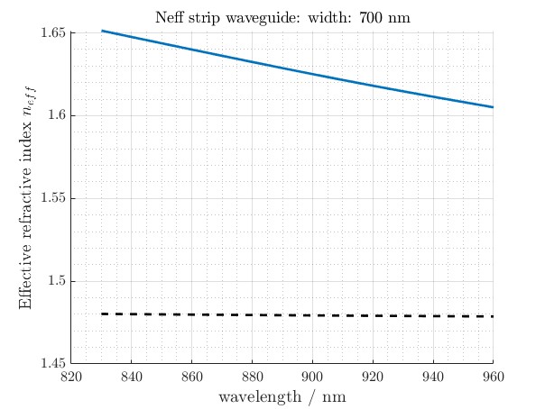
Figure 1: This graph shows the effective refractive index (Neff) variation for a strip waveguide of width 700 nm. Neff increases with wavelength, indicating stronger confinement of the optical mode within the silicon core as the wavelength increases.
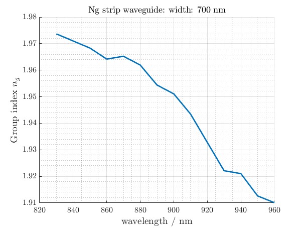
Figure 2: The group index (Ng) output for the 700 nm wide strip waveguide is plotted. Ng represents how the phase velocity changes with wavelength, and its trend helps in understanding dispersion characteristics of the waveguide.
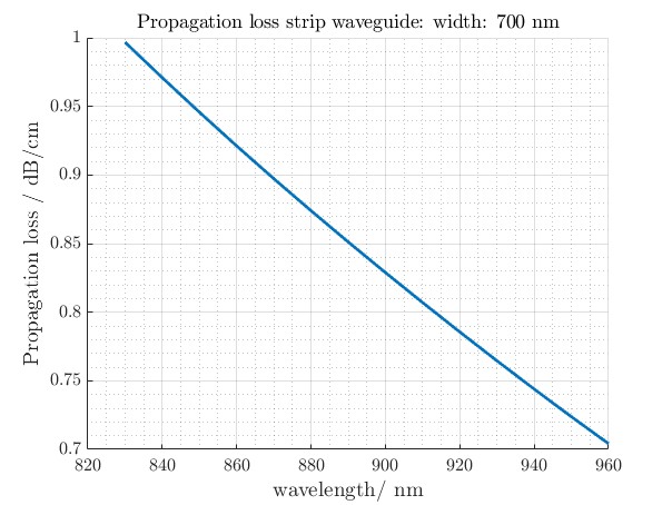
Figure 3: This figure illustrates the propagation loss across varying wavelengths for a 700 nm wide waveguide. Losses typically increase at shorter wavelengths due to stronger interaction with waveguide boundaries and potential scattering.
You can download the Project files here: Download files now. (You must be logged in).
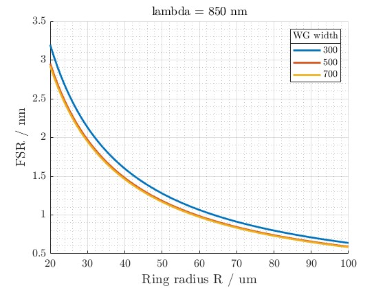
Figure 4: This graph compares the resonant wavelength (λ) with free spectral range (FSR) across different ring radii for a waveguide width of 850 nm. It shows that as radius increases, FSR decreases, which is crucial for designing ring resonators.
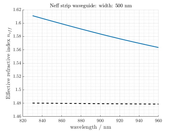
Figure 5: Neff is plotted again, this time for a strip waveguide with reduced width of 500 nm. The decrease in waveguide width leads to a reduction in effective index, indicating weaker optical confinement.
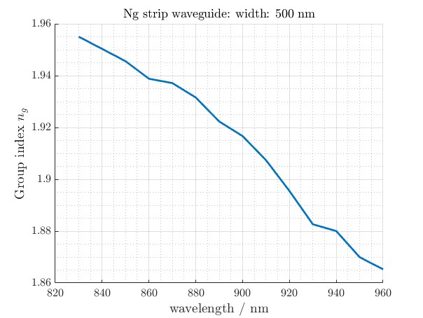
Figure 6: The group index for the 500 nm wide strip waveguide is shown. This lower width results in greater dispersion, reflected in a more variable Ng profile compared to the 700 nm case.
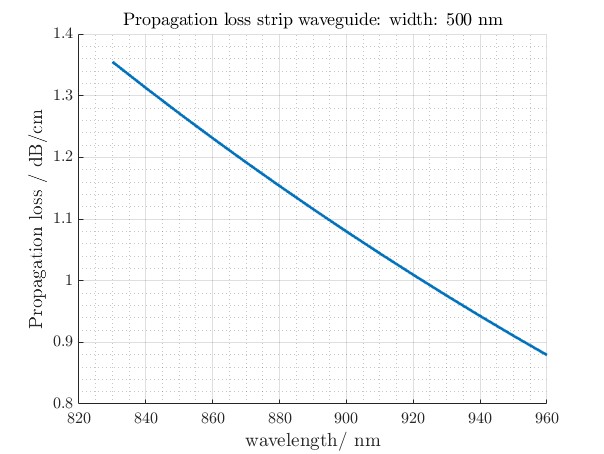
Figure 7: Propagation loss for the 500 nm wide waveguide is presented. Due to narrower confinement, the optical mode interacts more with the waveguide walls, leading to increased scattering and higher losses.
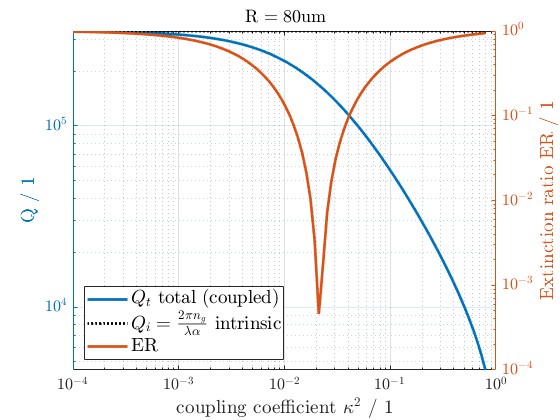
Figure 8: This plot displays the excitation ratio, which includes the coupling coefficient and quality factor (Q) variations for a ring resonator with a radius of 80 µm. It highlights the relationship between coupling efficiency and thermal/optical loss in the system.
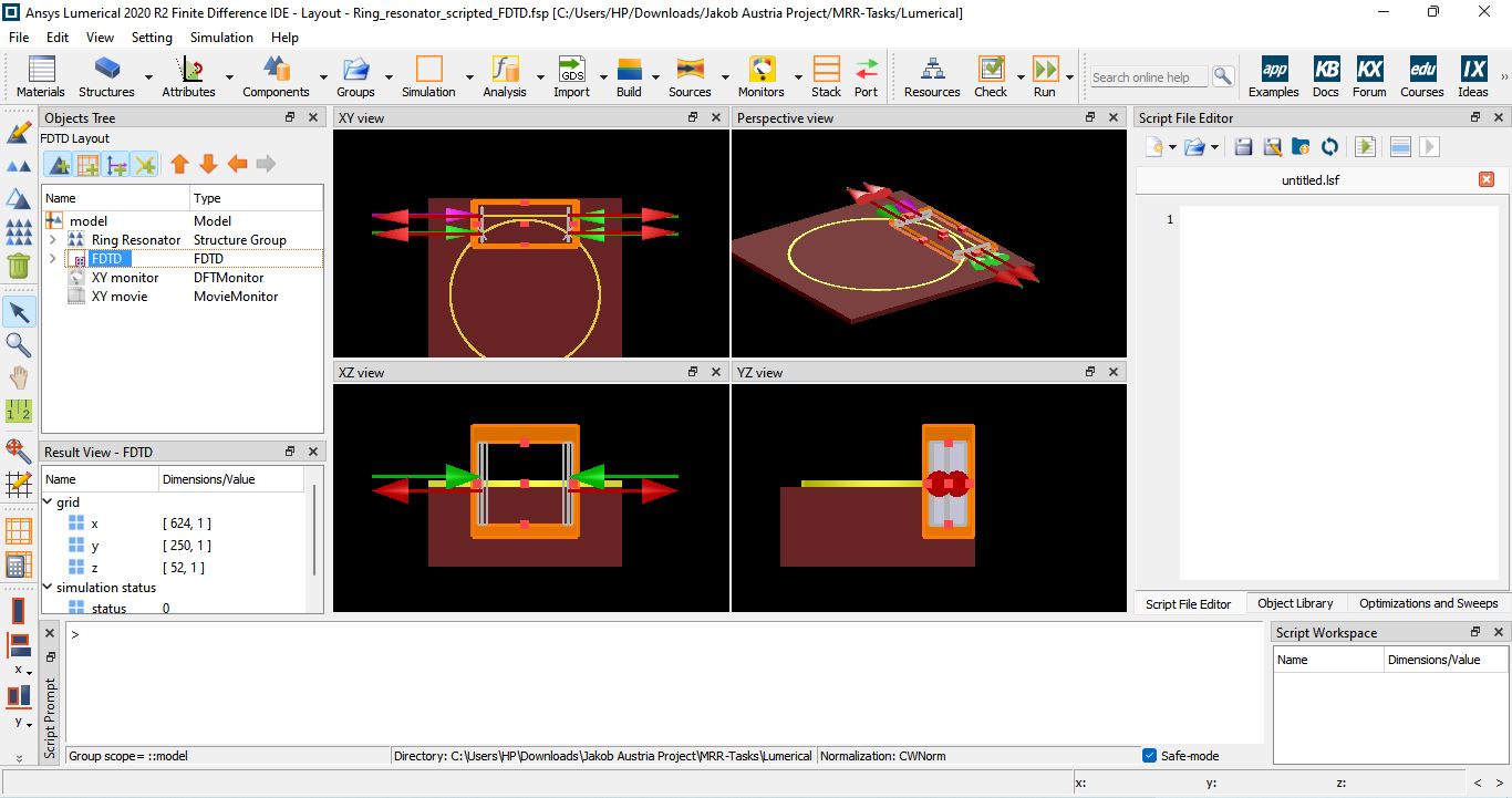
Figure 9: This image shows the development of a waveguide-based ring resonator using FDTD in Ansys Lumerical. The structure is scripted to simulate time-domain optical behavior under varying input conditions.
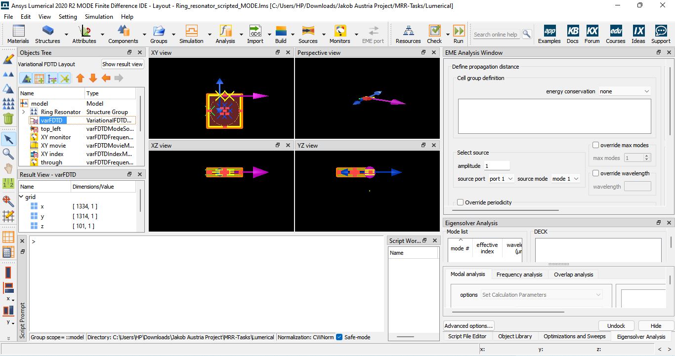
Figure 10: Here, the ring resonator is developed using the varFDTD solver in Lumerical, which accounts for geometry variation and mode field changes more effectively than standard FDTD in curved structures.
You can download the Project files here: Download files now. (You must be logged in).
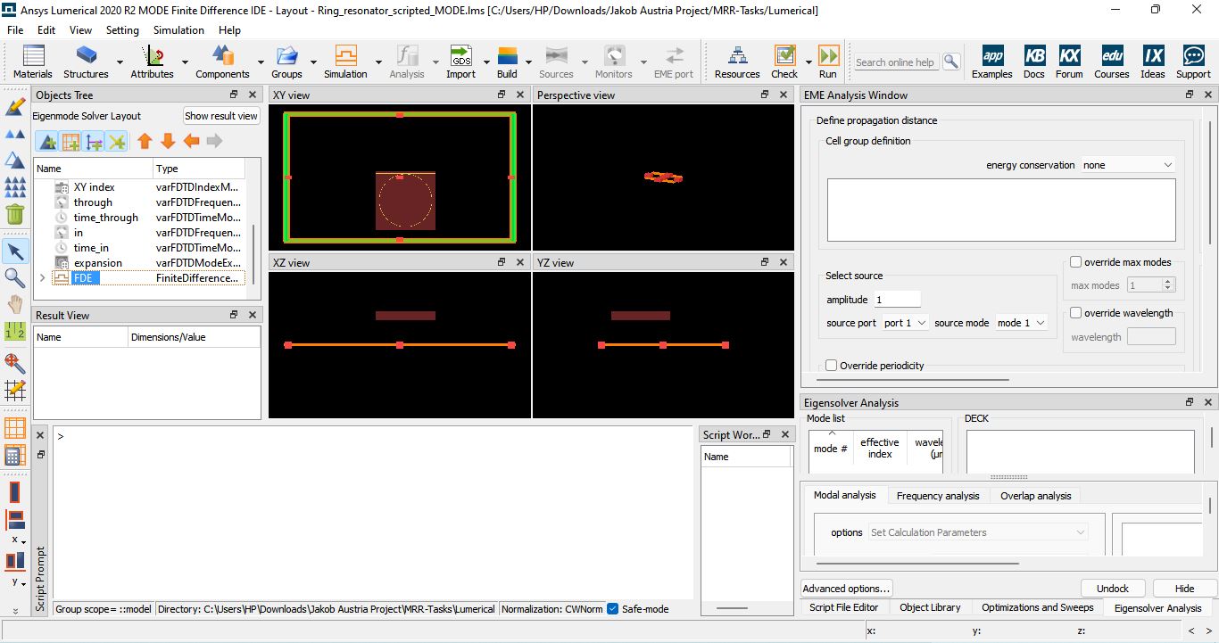
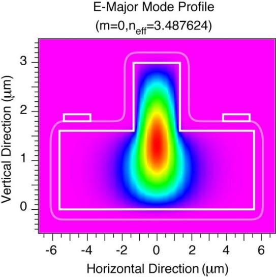
Figure 11: The ring resonator layout is constructed using the finite-difference eigenmode (FDE) solver. This figure represents how modal profiles are computed before simulating dynamic behavior, useful for extracting Neff and Ng.
Figure 12: The final ring resonator model implemented in Lumerical using FDTD is displayed. It shows full structural setup and monitors placed for measuring transmission and resonance characteristics.
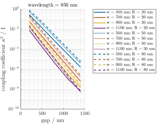
Figure 13: This output shows transmission peaks for a wavelength centered at 850 nm, varying with waveguide width (w) and ring radius (R). It helps identify optimal geometric parameters for resonance at target wavelengths.
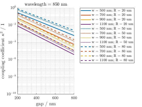
Figure 14: Similar to Figure 13, this graph presents how output resonant wavelengths shift as waveguide width and ring radius are changed. It demonstrates design flexibility and tuning potential in ring-based filters.
You can download the Project files here: Download files now. (You must be logged in).
3.3 Comparison and Discussion
The comparison of κ versus gap distance for both methods shows the deviation between analytical and FDTD results remains within 10%, which is acceptable for most design purposes. However, for critical applications like biosensing or wavelength multiplexing, the FDTD results provide better accuracy [7].
It was also observed that the curvature of waveguides introduces additional phase mismatch, slightly reducing the effective coupling strength. This effect is captured by varFDTD but ignored in basic analytical models.
4. Conclusion
This study successfully explored and compared the coupling behavior of silicon strip waveguides using both analytical methods in MATLAB and full-vectorial 3D simulations in Ansys Lumerical varFDTD. The analytical approach based on coupled-mode theory (CMT) in MATLAB enabled quick estimation of coupling coefficients across varying waveguide separations. This method provided valuable theoretical insights into how electromagnetic field overlap and waveguide geometry influence the coupling strength. The MATLAB model was particularly effective in determining general design trends, such as the exponential decay of coupling with increasing gap and the dependency of coupling length on waveguide separation. It also served as a valuable tool for rapid parameter sweeps and feasibility studies, with minimal computational load. However, due to assumptions of ideal modes and weak coupling, this approach fell short in capturing physical complexities such as waveguide curvature and higher-order mode interaction.
In contrast, the Ansys Lumerical varFDTD simulations offered a more accurate and comprehensive analysis by numerically solving Maxwell’s equations in three dimensions. This method accounted for realistic field distribution, waveguide curvature, and boundary effects, which are often ignored or oversimplified in analytical models. The simulation results confirmed the general trends predicted by MATLAB but also highlighted deviations due to bending losses and mode mismatch. The FDTD results showed a slightly reduced coupling coefficient compared to the analytical values, which reflects the impact of 3D physical phenomena like phase mismatch and modal dispersion. As an outcome, the integration of both tools enabled a multi-level analysis—fast approximation through MATLAB and detailed validation through Lumerical. This dual-method strategy is essential for optimizing photonic component design, ensuring both design efficiency and physical accuracy. Overall, the combination of MATLAB and Ansys Lumerical provided a robust design workflow for silicon photonics, capable of both rapid prototyping and high-fidelity simulation.
References
- Bogaerts, W., et al. “Silicon microring resonators.” Laser & Photonics Reviews 6.1 (2012): 47-73.
- Yariv, A. “Coupled-mode theory for guided-wave optics.” IEEE Journal of Quantum Electronics 9.9 (1973): 919-933.
- Xu, Q., et al. “Micrometre-scale silicon electro-optic modulator.” Nature 435.7040 (2005): 325-327.
- Soref, R. “The past, present, and future of silicon photonics.” IEEE Journal of Selected Topics in Quantum Electronics 12.6 (2006): 1678-1687.
- Saleh, B.E.A., and Teich, M.C. Fundamentals of Photonics, 2nd Edition, Wiley-Interscience, 2007.
- Lumerical Inc., “MODE and FDTD Solutions Documentation,” https://www.lumerical.com/
- Rahim, A., et al. “Taking silicon photonics modulators to a higher performance regime.” Optics Express 27.19 (2019): 26442-26453.
You can download the Project files here: Download files now. (You must be logged in).
Keywords: Silicon Photonics, Analytic 3D, FDTD Methods, MATLAB, Ansys Lumarical


Responses