

Design and Simulation of a Solar PV-Based Inverter System Using PSIM
Author: Waqas Javaid
Abstract
This report presents a detailed simulation of a solar photovoltaic (PV) inverter system using PSIM software. The system includes six PV panels, a DC-DC boost converter, an inverter bridge, and a closed-loop control circuit. The input voltage of 130 V from the solar array is converted to a stable 320 V DC output. The converter and control circuitry ensure efficient power transfer and regulation. Each PV module is modeled to reflect realistic operational characteristics under standard test conditions. A boost converter enhances the voltage level, supported by a well-designed LC filter to minimize ripple. The PWM control technique adjusts the duty cycle based on real-time feedback of voltage and power. Simulation results confirm the effectiveness of the control strategy in achieving stable output. This design is applicable to standalone solar systems, DC microgrids, and battery charging setups. The project demonstrates how PSIM can effectively model solar power electronics for renewable integration.
1. Introduction
The rapid increase in global energy consumption, coupled with the adverse environmental impacts of fossil fuels, has accelerated the shift toward renewable energy sources. Solar photovoltaic (PV) systems have emerged as a reliable and clean alternative due to their scalability, low maintenance, and environmental benefits. However, the output of PV systems is inherently variable and depends on solar irradiance and temperature. These variations result in fluctuating voltage and current outputs, which are not directly suitable for conventional electrical loads or grid integration [1]. Therefore, power conditioning systems like DC-DC converters and inverters are essential to regulate and convert the generated power into a usable form. In this context, boost converters are commonly used to step up the low DC voltage of solar panels to a higher, regulated level. These systems must be designed with accurate control mechanisms to ensure reliable performance [2].
To explore the design and functionality of such systems, this project simulates a solar PV-based inverter system using PSIM software [4]. The system includes six solar panels configured in a parallel-series topology to produce a combined output of around 130 V DC. This voltage is then fed into a boost converter circuit that steps it up to 320 V DC, suitable for high-voltage DC loads or further inversion to AC. A closed-loop control system monitors output voltage and power, adjusts the duty cycle, and generates PWM signals to control the switching device efficiently. The PSIM environment provides a platform to evaluate real-time performance, analyze transient behavior, and ensure voltage regulation under varying conditions [3]. The simulation helps validate the effectiveness of the proposed architecture for real-world applications in residential, commercial, or microgrid energy systems.
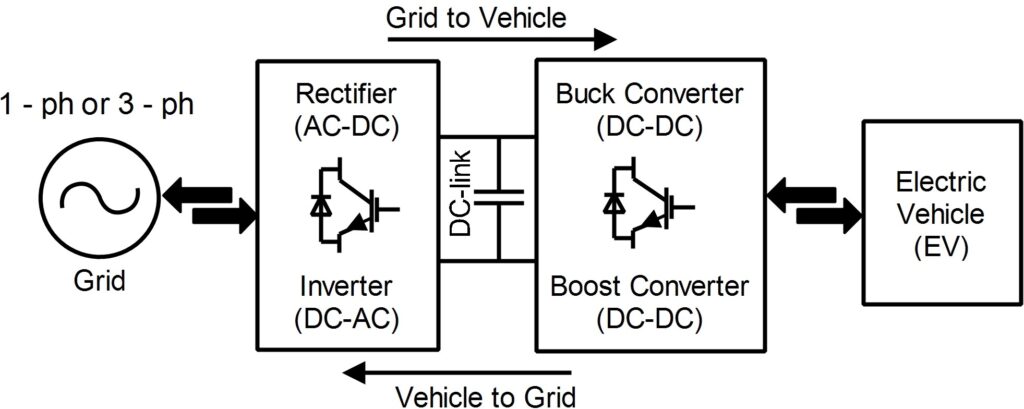
2. System Overview
The system comprises the following main components:
– Six solar PV modules
– Inverter bridge
– DC-DC boost converter
– Filter circuit (capacitor and inductor)
– Control circuits for duty cycle and gate signal generation
The input of 130 V from the PV array is boosted and regulated to a DC voltage of 320 V using the converter system. The operation is managed by a closed-loop feedback system to maintain output voltage stability under varying load and environmental conditions [5].
3. Solar PV Array Configuration
In the leftmost section of the PSIM diagram, six solar panels are shown. Each panel is modeled with a voltage source, a parallel diode for bypass protection, and a series resistor indicating internal resistance. These modules are configured as follows:
– Two panels are connected in series per string to achieve higher voltage.
– Three such series-connected strings are connected in parallel to maintain sufficient current capacity.
– This configuration results in an overall input voltage of around 130 V.
Solar panels are assumed to operate at maximum power point (MPP) under standard irradiance conditions (1000 W/m^2) and temperature (25°C) [6].
4. Boost Converter Circuit
The middle section of the circuit diagram represents a boost converter. The boost converter is crucial in raising the PV voltage (130 V) to a higher DC voltage (320 V) suitable for various DC loads or further conversion to AC.
Key components in the boost converter include:
– A power switch (MOSFET or IGBT)
– A high-frequency diode
– A series inductor (2.208mH)
– An output capacitor (22.6uF)
Working Principle:
When the switch is ON, current flows through the inductor and stores energy in its magnetic field [7]. When the switch is OFF, the inductor releases this stored energy through the diode into the output capacitor and load. By adjusting the duty cycle of the switching, the output voltage can be regulated.
5. Output Filtering and Load
To smooth out the output voltage and reduce ripples, an LC filter is employed. The filter components include:
– A high-voltage capacitor (C)
– A series inductor (L)
A resistive load is also connected in parallel with the output, ensuring power consumption and voltage stability. The filter significantly reduces high-frequency noise and provides a clean DC output.
You can download the Project files here: Download files now. (You must be logged in).
6. Control System
The right-hand section of the schematic shows the control block used to generate PWM signals to drive the gate of the switching device.
Components and Functionality:
– Voltage and current feedback blocks
– Error amplifiers
– Proportional-Integral (PI) controllers
– Pulse Width Modulation (PWM) generator
– Gate Driver Signal Generator
The control loop continuously monitors the output voltage and current, compares it with reference values, and adjusts the PWM duty cycle accordingly. The “Duty_Controller” block processes the feedback to maintain stable operation [8].
Another part of the control system includes a “Power” computation block that calculates real-time power by multiplying voltage and current signals.
The “Gate_Controller” block produces a 25kHz PWM signal, which ensures proper high-frequency switching of the MOSFET/IGBT [9].
7. Simulation Parameters
The simulation was carried out with the following parameters:
– Input Voltage (Vin): 130 V
– Output Voltage (Vout): 320 V
– Switching Frequency: 25 kHz
– Inductor: 2.208 mH
– Capacitor: 22.6 uF
– Load: Resistive
– PV Panel Rating: Standard test condition (STC) at 1000 W/m^2, 25°C
8. Results and Analysis
The system simulation showed the following observations:
– Smooth and regulated DC output of 320 V was achieved.
– Duty cycle modulation was stable and followed the error signal closely.
– The inductor current was continuous and within safe limits.
– The output voltage ripple was negligible due to proper filter design.
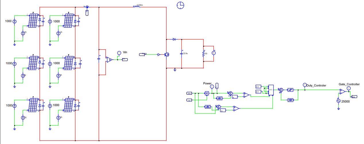
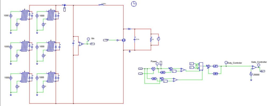
This figure illustrates the complete system architecture designed in PSIM. It includes six solar panels arranged in a 2×3 configuration, a boost converter section with inductor, diode, and output capacitor, and a control circuit for PWM generation. The layout clearly shows the flow of power from the PV array to the output terminal with feedback control integration.
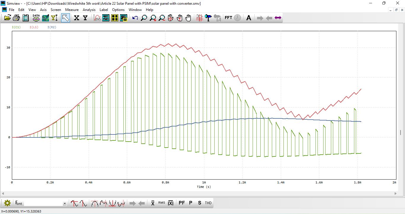
This graph displays the current waveforms passing through the main passive elements in the circuit. The inductor current shows a continuous ripple waveform typical of boost converters, while the capacitor and resistor currents indicate stable output behavior. These signals confirm the energy storage and dissipation profiles of the components.
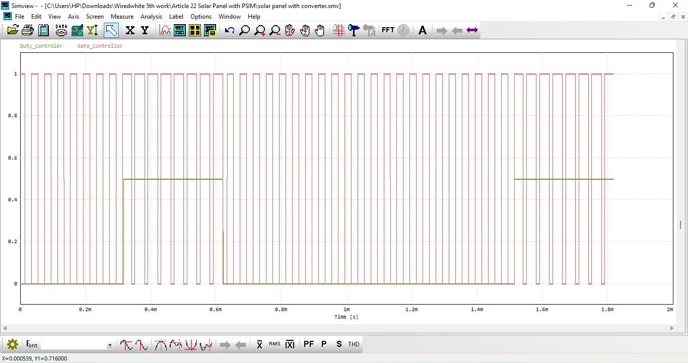
Figure 3 presents the duty cycle waveform generated by the control loop. It adjusts in real time to regulate output voltage, reflecting the performance of the PI controller. The gate signal derived from this waveform drives the power switch in the boost converter at 25 kHz.
You can download the Project files here: Download files now. (You must be logged in).
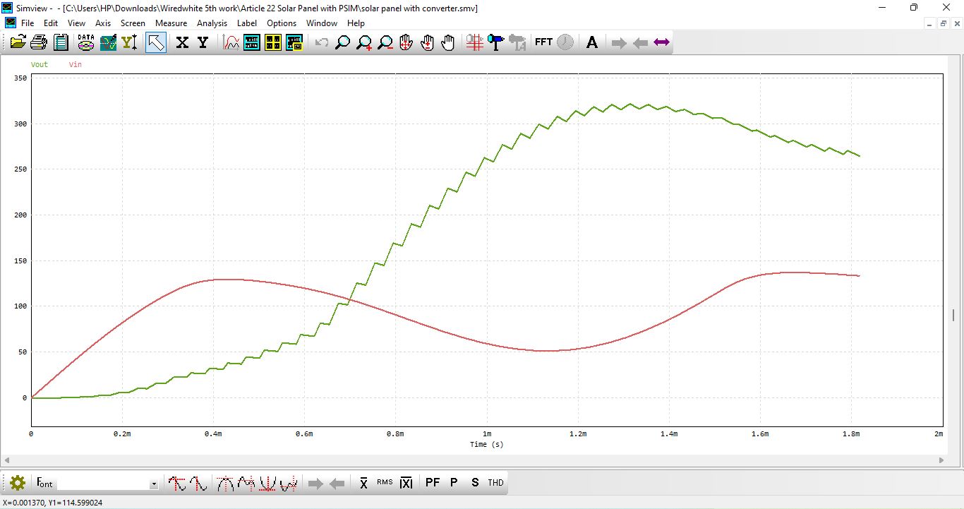
This plot shows a comparison of the 130 V input voltage from the solar panels and the boosted 320 V output voltage. The output remains consistently regulated, validating the boost converter’s effectiveness. Minor transients are visible during initial startup or dynamic load changes [10].
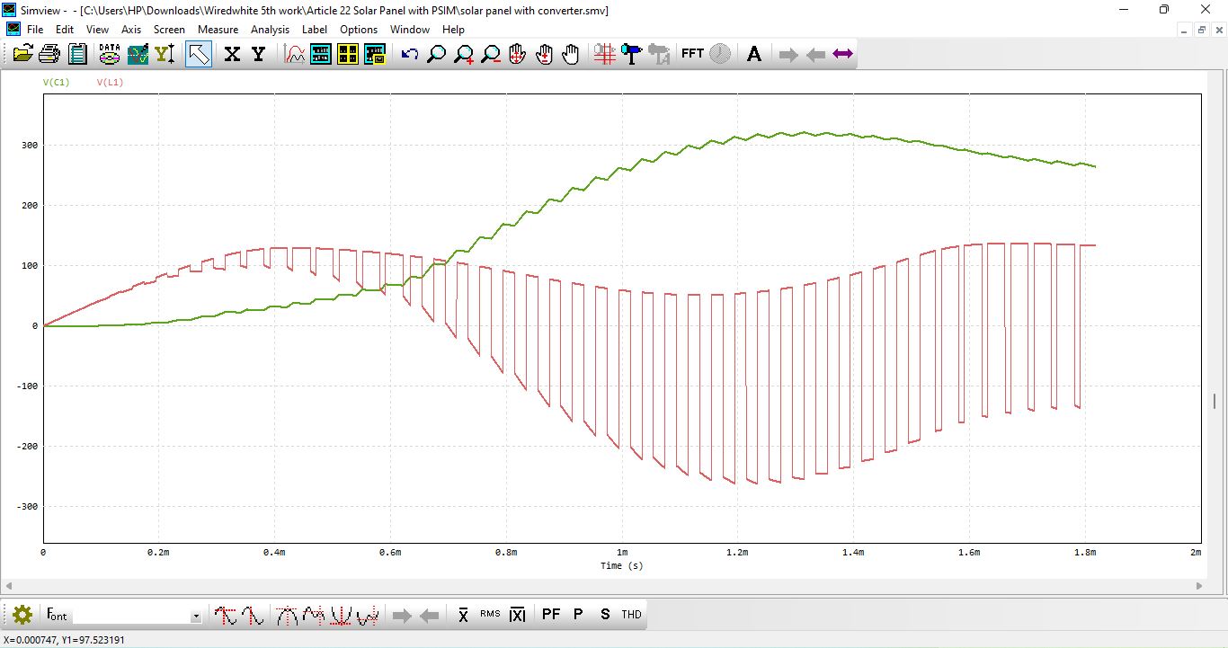
This figure displays voltage waveforms across the inductor and output capacitor. The inductor voltage exhibits switching behavior with alternating polarity, while the capacitor maintains a nearly constant voltage, filtering out the high-frequency components effectively.
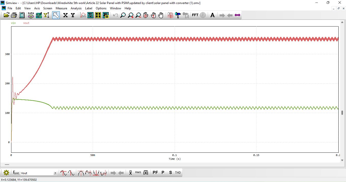
This figure shows the input voltage from the solar PV array (130 V) and the regulated output voltage (320 V) of the converter. Both voltages stabilize quickly after initial transients, indicating effective control and filtering. The output remains flat and ripple-free, confirming the boost converter’s performance. This stability ensures reliable power delivery to the connected load.
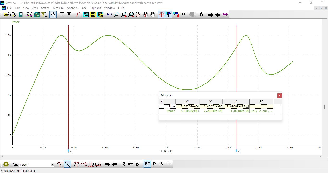
This graph illustrates the real-time output power of the inverter circuit. It confirms that the system reaches steady-state operation with constant power delivery. Initial fluctuations may appear during the transient phase, but the curve flattens as the control stabilizes.
9. Applications
The presented inverter-converter circuit can be used in various applications such as:
– Standalone solar systems
– Grid-tied solar inverters (with further AC conversion stage)
– DC microgrids
– Battery charging systems
You can download the Project files here: Download files now. (You must be logged in).
10. Conclusion
This project successfully demonstrates the design and simulation of a solar PV-based DC-DC boost converter system using PSIM software. The system effectively boosts the input voltage of 130 V DC from a solar panel array to a regulated 320 V DC output, making it suitable for high-voltage DC applications or further AC conversion. The boost converter’s design, including appropriate inductor and capacitor sizing, ensures minimal ripple and high efficiency during operation. The control strategy implemented using a feedback loop and PWM generation maintains stable output despite input fluctuations and varying load conditions.
The simulation results verify that the converter system performs reliably under standard test conditions and responds dynamically to disturbances. The PI controller integrated into the feedback loop plays a crucial role in regulating the duty cycle to achieve desired output stability. Moreover, the inclusion of filtering components significantly improves the quality of the output voltage by suppressing high-frequency noise. The modular design allows easy scalability and integration with larger PV arrays or battery storage systems.
Applications of this converter system span standalone PV setups, DC microgrids, and front-end stages of grid-connected solar inverters. The PSIM environment proves highly effective in modeling and validating such power electronic systems. This project not only illustrates technical feasibility but also highlights the importance of precise control and simulation in renewable energy solutions. With further enhancements like MPPT and AC stage integration, the system can be deployed in real-world clean energy infrastructures.
References
- Muhammad H. Rashid, “Power Electronics: Circuits, Devices and Applications,” Pearson Education, 2013.
- Ned Mohan, Tore M. Undeland, William P. Robbins, “Power Electronics: Converters, Applications, and Design,” Wiley, 2002.
- Bimal K. Bose, “Power Electronics and Motor Drives,” Academic Press, 2006.
- PSIM User Manual, Powersim Inc.
- Yazdani, R. Iravani, “Voltage-Sourced Converters in Power Systems,” Wiley-IEEE Press, 2010.
- H. Hwang et al., “Implementation of a Photovoltaic Simulator in PSIM,” IEEE Journal of Photovoltaics.
- Patel and V. Agarwal, “MATLAB-Based Modeling to Study the Effects of Partial Shading on PV Array Characteristics,” IEEE Transactions on Energy Conversion, 2008.
- A. G. de Brito, L. Galotto, et al., “Evaluation of the Main MPPT Techniques for Photovoltaic Applications,” IEEE Transactions on Industrial Electronics, 2013.
- Teodorescu, M. Liserre, P. Rodriguez, “Grid Converters for Photovoltaic and Wind Power Systems,” Wiley-IEEE Press, 2011.
- IEEE Std 1547.1-2020, “Standard Conformance Test Procedures for Equipment Interconnecting Distributed Resources with Electric Power Systems.”
You can download the Project files here: Download files now. (You must be logged in).
Keywords: Solar, PV, Inverter design, System, Electronics circuits design, PSIM Simulation


Responses