

Analysis and Hardware Implementation of 3-Level and 5-Level CHB Multilevel Inverters Using SPWM

1. INTRODUCTION
1.1 Inverter
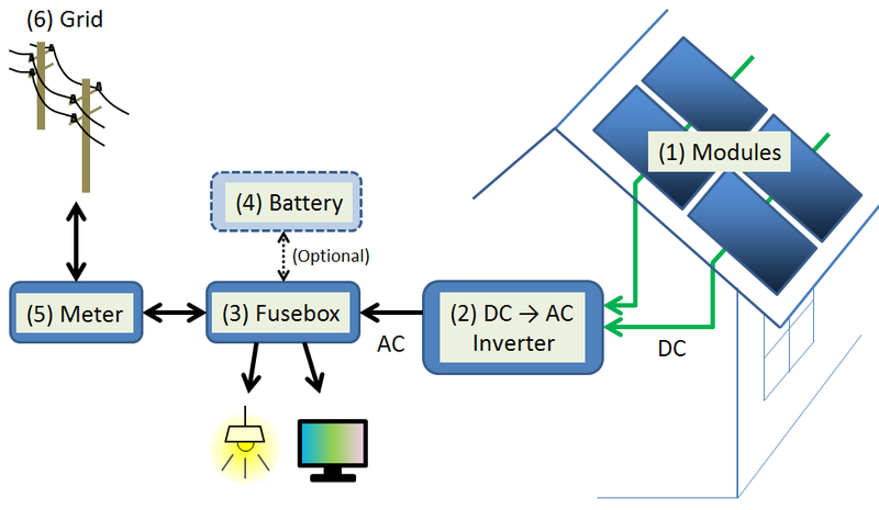
Inverters are power electronic devices that regulate the flow of electrical power. An inverter converts the DC voltage to an AC voltage. The batteries in the inverter store energy in the form of direct current and the home appliances we use need alternating current. The inverter can be utilized to power our appliances during such emergencies as power outages.
1.2 Working of an inverter
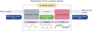
Converter circuit used in the front part constantly converts alternating current to direct current. This process is called rectification. Diode is used to pass electricity in a forward direction to convert it into direct current, but not in the reverse direction [1].
Diode’s structure is shaped like a bridge so that it can pass the negative peak in a forward direction. This is called full-wave rectification due to the fact that it transforms both the forward and negative wave peaks. Ripple voltage fluctuations will remain, in order to clean this up the capacitor is repeatedly charged and discharged, gently smoothing and changing the waveform close to that of direct current.
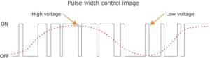
The inverter circuit then outputs alternating current with varying voltage and frequency. The DC/AC conversion mechanism switches power transistors such as “IGBT (Insulated Gate Bipolar Transistor) and changes the ON/OFF intervals to create pulse waves with different widths. This is called Pulse Width Modulation (PWM).
1.3 Difference between UPS and Inverter
- The primary purpose of a UPS is to store electrical power, whereas an inverter transforms AC power into DC power.
- In the event of a power failure, the UPS will switch from mains to battery immediately, but the inverter will be delayed for a time.
- UPS connects directly to the appliance, while the inverter is first connected to the battery and then to the appliance circuit.
1.4 Types of inverters
The Single-phase inverters are divided into two types:
- Half-bridge inverter
- Full-bridge
Half Bridge Inverter:
It consists of two switches, voltage sources of voltage equal to Vdc/2. The switches are balanced with each other so that when one switch is activated, another switch is automatically deactivated [2].
Full Bridge Inverter:
A full-bridge inverter circuit converts direct current to alternating current. The components required for conversion are two times more than that used in single phase Half bridge inverters. The output will be equal to the given input i.e. Vdc.
1.5 Applications of an inverter
The inverter is used for emergency backup in case of power failure. It turns on electrical appliances when the main power is turned off. They are used in many applications such as:
- Small car adapters for offices, home applications, large grid systems, solar power
systems.
- UPS-Uninterruptible power supplies
- An inverter is the basic building block of an SMPS- switched mode power
- These can be used in Centrifugal fans, pumps, mixers, extruders, test stands, conveyors, metering pumps and Web-handling equipment.
2. MULTILEVEL INVERTER
2.1 Definition
Some devices in industries require medium or low power to operate. Using a high power source for all industrial loads can be beneficial for some high power motors, while it can be detrimental to others. The multi-level inverter is like an inverter that provides high output power from a medium voltage source such as batteries, super capacitors, and solar panels [3].
The multi-level inverter (MLI) is an improved form of a two-stage inverter. In a multi-level inverter we do not process two-level voltage instead in order to create a smoother stepped output waveform, more than two voltage levels are combined together. The smoothness of the waveform is proportional to the voltage levels, as we increase the voltage level the waveform will be smoother but the circuit complexity will increase.
2.2 Difference between inverter and multilevel inverter
In recent years, more attention has been paid to high power multistage converters. Better power quality, smaller output filter, lower output dv/dt stress, increased modularity and reliability, and use of low voltage semiconductors in high voltage applications These are just a few of the advantages of these converters over conventional two- or three-level converters.
| Sl. No | Conventional Inverter | Multilevel Inverter |
| 1. | THD is high in the output waveform | THD is low in the output waveform |
| 2. | High Switching stresses | Low Switching stresses |
| 3. | Not used for high Voltage applications | Used for High voltage applications |
| 4. | High voltage levels cannot be produced | Low voltage levels cannot be produced |
| 5. | High dv/dt and EMI | Low dv/dt and EMI |
| 6. | High switching frequency, increased switching losses | Lower switching frequency, reduced switching losses |
2.3 Different structures of multilevel inverter
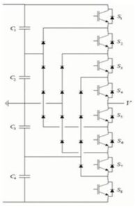
A. Diode Clamped Multilevel Inverter:
The main concept of this inverter is to use diodes and provide the multiple voltage levels through the different phases to the capacitor banks which are in series. A diode transfers a limited amount of voltage, thereby reducing the stress on other electrical devices. The maximum output voltage is half of the input DC voltage. It is the main drawback of the diode clamped multilevel inverter [4].
This problem can be solved by increasing the switches, diodes, and capacitors. Due to the capacitor balancing issues, these are limited to the three levels.
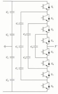
B. Flying Capacitors Multilevel Inverter:
The main concept of this inverter is to use capacitors. It is of a series connection of capacitor clamped switching cells. The capacitors transfer the limited amount of voltage to electrical devices. In this inverter switching states are like in the diode clamped inverter. Clamping diodes are not required in this type of multilevel inverters [7]. The output is half of the input DC voltage. It is a drawback of the flying capacitors multilevel inverter. It also has the switching redundancy within the phase to balance the flying capacitors. It can control both the active and reactive power flow. But due to the high-frequency switching, switching losses will take place.
EX: 5-level flying capacitors multilevel inverter
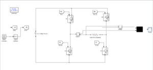
3. CASCADED H- BRIDGE INVERTER
3.1 Structure
One of the basic and well-known topologies among all multilevel inverters is Cascaded H-Bridge Multilevel Inverter. It can be used for both single and three phase conversion. It uses H-Bridge including switches and diodes [8].
The modulation technique that applies to each cell of the inverter may be the same or different. It varies from fundamental switching frequency PWM, carrier based PWM or combination of the two different PWM methods (known as mixed / hybrid PWM method). In this project we are using Level Shifted PWM. Level Shifted PWM uses some carrier signals, which are arranged in different levels among the carriers.
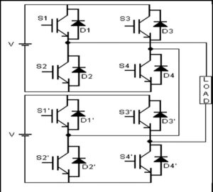
Each H-Bridge Cell consists of four switches and four diodes as shown in the Fig 5.
- Like every H-Bridge, different combinations of switch positions determine different voltages such as V+, V- and 0.
- Two switching combinations are present for 0
- S1 and S3 are connected to positive voltage and S2 and S4 are connected to negative
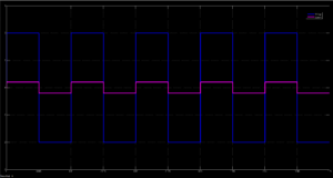
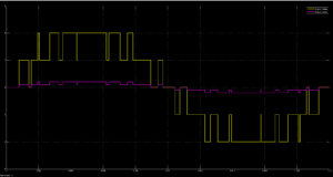
3.2 Working of 3- level H-bridge inverter
Pulse given to the switch S2 is delayed by T/4 sec when compared to switch S1. And the switches in the same branch have inverted pulses so that there won’t be any short circuit.
The switching pattern and the output voltage is given in the below table.
Table 1: Switching pattern and output voltages
| Switches States | Output Voltage | |||
| S1 | S2 | S3 | S4 | |
| ON | OFF | ON | OFF | 0 |
| ON | ON | OFF | OFF | Vdc |
| OFF | OFF | ON | ON | -Vdc |
| OFF | ON | OFF | ON | 0 |
3.3 Advantages of Cascaded H-Bridge Multilevel Inverter
- It needs less number of components compared with diode clamped and flying capacitor inverters. Soft-switching is possible by some of the new switching methods.
- They are used to eliminate the bulky transformer required in case of conventional multi-phase inverters, clamping diodes required in case of diode clamped inverters and flying capacitors required in case of flying capacitor inverters. But these require a large number of isolated voltages to supply each cell [5].
- The total number of output voltage levels is more than twice that of the number of DC sources available.
- The use of separate DC sources provides isolation of between sources of each
- Since the outputs of all the modules gets added, the voltage rating of individual modules is low and hence stress on individual devices also gets reduced.
You can download the Project files here: Download files now. (You must be logged in).
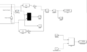
4. SIMULATIONS AND OBSERVATIONS
4.1 Half Bridge Inverter
Input Parameters:
T = 0.01s V1 = 2V V2 = 2V
Duty Cycle = 50% R = 10 ohm
4.2 Full Bridge Inverter
Input Parameters:
T = 0.01s V1 = 2V
Duty Cycle = 50% R = 10 ohm
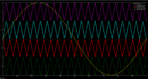
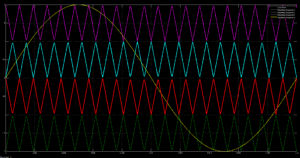
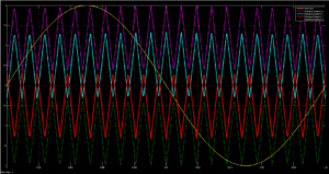
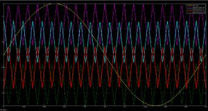
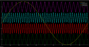
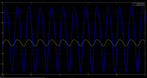
4.3 5-level SPWM inverter
Input Parameters:
T= 0.02s V1 = 2V V2 = 2V
R=10 ohm
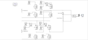
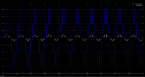
4.5 5-level SPWM inverter
Input Parameters:
T= 0.02s V1 = 2V V2 = 2V
R=10 ohm
Pulse width modulation type: Level Shifted
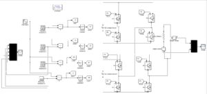
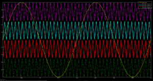
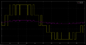
Table 2: Comparison table of Carrier wave frequency vs. THD(%) [2]
| Carrier frequency (Hz) | 3-Level | 5-Level |
| 19*50 | 51.91 | 26.61 |
| 20*50 | 55.07 | 27.43 |
| 21*50 | 50.8 | 26.87 |
| 22*50 | 53.36 | 27.5 |
| 23*50 | 53.46 | 26.99 |
| 24*50 | 50.42 | 26.28 |
| 25*50 | 54.94 | 27.41 |

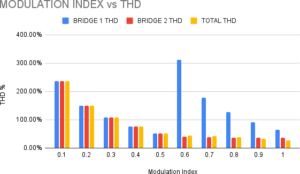
Table 3: Comparison table of modulation index and THD [4][5]
| Modulation Index | Bridge 1 | Bridge 2 | Total THD | |||
| THD | Amplitude | THD | Amplitude | THD | Amplitude | |
| 0.1 | 236.33% | 3.856e-05 | 236.33% | 0.1928 | 236.33% | 0.1928 |
| 0.2 | 149.28% | 8.138e-05 | 149.28% | 0.407 | 149.28% | 0.4069 |
| 0.3 | 108.53% | 0.001177 | 108.53% | 0.5887 | 108.53% | 0.5886 |
| 0.4 | 76.81% | 0.0001597 | 76.81% | 0.7988 | 76.81% | 0.7987 |
| 0.5 | 51.28% | 0.0002024 | 51.28% | 1.012 | 51.28% | 1.012 |
| 0.6 | 312.72% | 0.09628 | 41.24% | 1.103 | 44.47% | 1.2 |
| 0.7 | 178.36% | 0.254 | 38.31% | 1.157 | 42.14% | 1.411 |
| 0.8 | 126.73% | 0.4154 | 36.36% | 1.183 | 38.48% | 1.598 |
| 0.9 | 91.89% | 0.598 | 35.73% | 1.204 | 33.58% | 1.802 |
| 1 | 64.96% | 0.7841 | 35.89% | 1.214 | 27.11% | 1.988 |
Amplitude modulation index (ma) = Vref / Vc,
where Vc and Vref are carrier and reference voltages respectively.
Frequency modulation index (mf) = fc / fref,
where fc and fref are carrier and reference frequencies respectively.
Both, the modulation index and the carrier frequency are affecting the harmonic contents of the inverter output voltage waveform. The frequency spectrums of the unwanted harmonics are shifted towards higher frequency by increasing the carrier frequency [2] [3]. The total harmonic distortion (THD) factor of the inverter output voltage decreases as the modulation index increases. For carrier frequencies, greater than a certain value, the THD factor doesn’t change much by further increasing the frequency of the carrier signal.

Vn is the rms value of nth harmonic, V1 is the value of the fundamental component, n is the low-order harmonics and r is the maximum harmonic included in the THD calculation [1].
4.6 Different Modulation Techniques
4.6.1 Phase Disposition
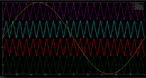
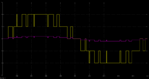
Fig 22 demonstrates the sine-triangle method for a five-level inverter where in modulation or sinusoidal reference signal is compared with four (m-1 in general) triangle waveform when the number of output voltage level is 5 (= m), 4 (m –1) carrier waveforms are arranged so that every carrier is in phase.
- The carriers are in phase across all the
- The frequency modulation index mf = fc / fm.
- The amplitude modulation index ma = 2Am / Az(m-1).
4.6.2 Phase Opposition and Disposition
For POD modulation all carrier waveforms above zero reference are in phase and they are 180 degrees out of phase with those below zero. When the number of levels is m ( = 5), m – 1 (= 4) carrier waveforms are arranged so that all carrier waveforms above zero are in phase and are 180° out of phase with those below zero. The significant harmonics are located around the carrier frequency for both the phase and line-to-line voltage. Formula for ma and mf are the same as that of PD PWM technique.
4.6.3 Alternative Phase Opposition and Disposition

In case of APOD modulation, every carrier wave is out of phase with its neighbor carrier by 180°. Since APOD and POD schemes in case of three level inverters are the same, a five level inverter is considered to discuss the APOD scheme. When the number of levels m (= 5) , m – 1 = 4 carrier waveforms are arranged so that every carrier waveform is out of phase with its neighbor carrier by 180°. Carriers in adjacent bands are phase displaced by 180° [2]. With this method, the most significant harmonics are centered as sidebands around the carrier. Formulas for ma and mf are the same as that of the PDPWM strategy.
You can download the Project files here: Download files now. (You must be logged in).
4.6.4 Carrier Overlapping PWM – A

In this case it can be seen that the four carriers are overlapped with each other and the reference sine wave is placed at the middle of the four carriers. The carrier waves are in same phase.
4.6.5 Carrier Overlapping PWM – B
In this case it can be seen that they are divided equally into two groups according to the positive/negative average levels. In this strategy, the two groups are opposite in phase with each other while keeping in phase within the group [3] [4].
4.6.6 Carrier Overlapping PWM – C
In this strategy, carriers invert their phase in turns from the previous one. It may be identified as PWM with amplitude overlapped and neighboring phase interleaved carriers.
4.6.7 Variable Frequency PWM

The number of switching for upper and lower devices of chosen MLI is much more than that of intermediate switches in above PWM strategies using constant frequency carriers. In order to equalize the number of switching’s for all the switches, VFPWM strategy is used in which the carrier frequency of the intermediate switches is properly increased to balance the numbers of switching for all the switches [4] [5]. In fig 34, the frequencies of carrier wave and sine wave are 41 and 21 respectively. The amplitude modulation index for VFPWM strategy is:
ma = 2Am / Ac(m-1).
| Modulation technique | Total Loss | Conduction Loss | Switching Loss | THD |
| Phase Disposition | 0.03424 | 2.009 e-5 | 0.03422 | 26.87% |
| Phase Opposition and Disposition | 0.03412 | 2.004 e-5 | 0.0341 | 26.91% |
| Alternative Phase Opposition and Disposition: | 0.03424 | 2.009 e-5 | 0.03422 | 26.88% |
| Carrier Overlapping PWM – A: | 0.04103 | 2.28 e-5 | 0.04101 | 33.96% |
| Carrier Overlapping PWM – B: | 0.04083 | 2.272 e-5 | 0.04081 | 33.17% |
| Carrier Overlapping PWM – C: | 0.03908 | 2.202 e-5 | 0.03905 | 24.95% |
| Variable Frequency PWM: | 0.03432 | 2.012 e-5 | 0.0343 | 26.71% |
Table 3: Comparison of different modulation techniques
4.7 Relation between THD and Power Factor
The total power factor is calculated as follows:
PFTOTAL = PF × PFTHD
PF = cos(θ)
Where PF = displacement power factor
θ = Difference between the phase of the voltage and the phase of the current (phase displacement) in degrees.
The displacement power factor is the ratio of true power to apparent power due to the phase displacement between the current and voltage
![]()
Where PFTHD = distortion power factor, THD = Total harmonic distortion
The presence of harmonics complicates the discussion of the power factor. The distortion power factor is the ratio of true power to apparent power due to THD. Hence, Lower THD in power systems means higher power factor [6] [7].
You can download the Project files here: Download files now. (You must be logged in).
5. DESIGN AND CALCULATIONS
5.1 Switch Loss Calculations
Total losses = conduction loss + switching loss Losses of 5 level SPWM:
Conduction loss = 2.009 e-5 Switching loss = 0.03422 Total loss = 0.03424
5.2 Filter Design and Calculations
LC Filter Design
Vin = 100v R = 10Ω
Vout(rms)=Vdc = 100v Vo = 100√2 sin wt Iout(rms) = 10 A
Pout = 1000 watt
Inductor design
ΔI = 20% of rated current = 2A ΔI ₐₓ = Vdc / (4XL FSW)
L = Vdc / (4 x ΔI0 0ₐₓ x Fsw) =100 / (4X2 x √2 x1000)
= 8.83mH
Capacitance design Fc = 1 / (2 x πX√LC) Fc <= F / 10
C = (10/2*π*F) ^2 * (1/L)
= (10/2*π*1000)^2 * (1/8.83*10^-3)
= 0.286mF
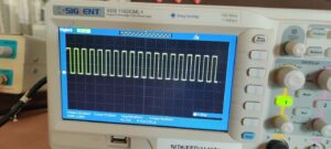
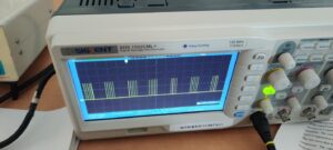
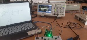
6. HARDWARE IMPLEMENTATION
6.1 Components used
Arduino UNO, MOSFETs -700N65P, H-bridges, pulse generator, DC Supply, Oscilloscope, Multimeter, Breadboard, Connecting wires.
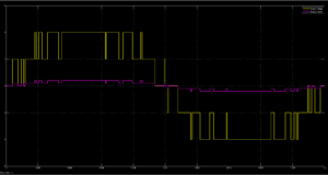
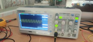
6.2 Testing Arduino UNO Output pins
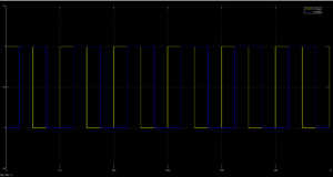
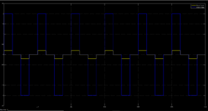
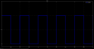
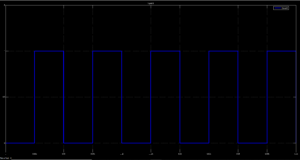
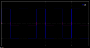
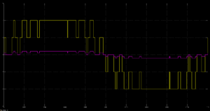
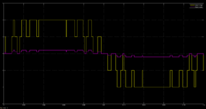
Out of 13 signal output pins of Arduino UNO 6 pins (pin nos 3, 5, 6, 9, 10, 11) are used for SPWM output. To test the output pins, a rectangular pulse and SPWM pulse is given as input to Arduino.
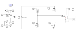
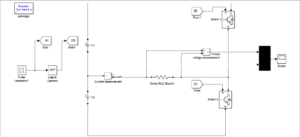
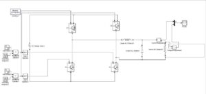
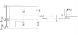
6.3 Circuit diagram
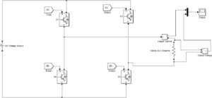
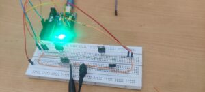
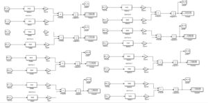
A 3 level CHB MLI is built using 4 Mosfets, breadboard and the connections are made according to Figure 28. The Mosfet gate triggering pulses are generated using MATLAB simulink and are loaded into Arduino UNO.
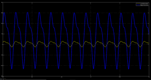
6.4 Input and output images
You can download the Project files here: Download files now. (You must be logged in).
7. CONCLUSION
In this project, different topologies of inverters such as full bridge, half bridge, cascaded h-bridge have been analyzed. 3 level and 5 level inverters have been analyzed with SPWM technique and different SPWM techniques have also been executed. After analysis we find that the THD values of SPWM inverters are less than the normal multilevel inverters [8]. It has been observed that with increase in levels in multilevel inverters and with increase in modulation index THD decreases till a certain point. As the THD decreases, the power factor is improved. The above output variations have been demonstrated. Simultaneously, 3-level CHB MLI with and without SPWM has been implemented on the Arduino UNO board.
8. REFERENCES
- https://www.elprocus.com/what-is-an-inverter-types-circuit-diagram-applications/
- https://www.elprocus.com/multilevel-inverter-types-advantages/
- https://microcontrollerslab.com/multilevel-inverters-types-applications/
- https://ieeexplore.ieee.org/abstract/document/9364104
- https://www.google.com/url?sa=i&url=https%3A%2F%2Fwww.irjet.net%2Farchives%2 FV5%2Fi3%2FIRJET-V5I3230.pdf&psig=AOvVaw2ewV2Bc0nLojFhhh2TxLHZ&ust= 1669136028576000&source=images&cd=vfe&ved=0CBAQjRxqFwoTCICb37Lev_sCF QAAAAAdAAAAABAE
- _Ser. Mater._Sci._Eng._105_012003.pdf
- Chinnapettai Ramalingam Balamurugan, S.P. Natarajan, R. Bensraj, B. Shanthi,”Review on Modulation strategies of Multi-Level Inverters”.
- Babaie, B. Karami and A. Abrishamifar, “Improved equations of switching loss and conduction loss in SPWM multilevel inverters,” 2016 7th Power Electronics and Drive Systems Technologies Conference (PEDSTC), Tehran, Iran, 2016, pp. 559-564, doi: 10.1109/PEDSTC.2016.7556921.
Keywords: 3-level CHB MLI, 5-level CHB MLI, Cascaded H-bridge, Inverter, Multilevel inverters, SPWM.
You can download the Project files here: Download files now. (You must be logged in).


Responses