

Design and LTSpice Simulation of a High-Efficiency Bidirectional Single-Phase EV Charger for Vehicle-to-Grid (V2G) Applications
Methodology:
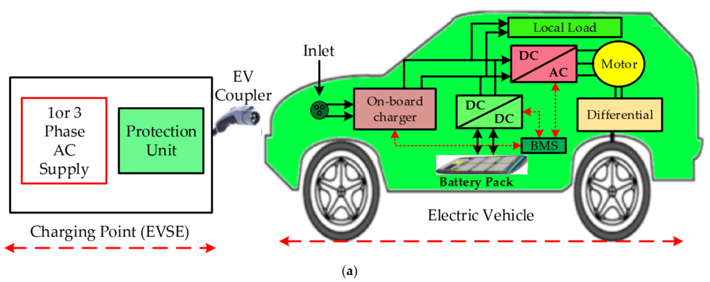
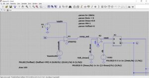
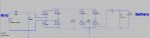
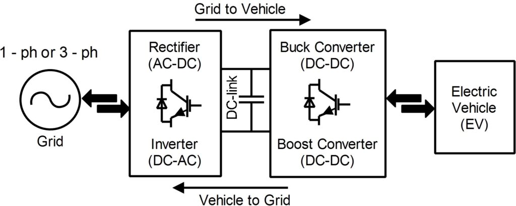
The methodology of the proposed single-phase bidirectional electric vehicle charger project centers on designing and simulating a highly efficient AC/DC converter system in LTSpice tailored for Vehicle-to-Grid (V2G) applications. The system architecture comprises an AC input of 230V, filtered using an LC filter to eliminate high-frequency harmonics, followed by a full-bridge converter operating at line frequency to enable bidirectional power flow. This converter rectifies the AC input to DC for charging the EV battery and inversely converts stored DC back to AC for grid feeding [3] [4]. A PWM-based control circuit manages the switching of H-bridge transistors, ensuring synchronization and efficient commutation. Downstream, an interleaved bidirectional buck-boost DC/DC converter regulates the battery voltage between 230V and 400V, depending on the charging or discharging mode. The interleaved structure minimizes current ripple, improving battery lifespan and performance. Simulation in LTSpice analyzes each stage’s operation, efficiency, current waveforms, and voltage levels to validate the system’s capability for efficient charging and seamless energy transfer back to the grid.
The methodology of the EV bidirectional charger particularly focusing on the input, output, and the key components mentioned.
- AC to DC Conversion:
- Input: AC 230 volts
- Full-bridge converter is used to rectify the AC input voltage to a DC voltage.
- The rectified DC voltage is likely used for charging the electric vehicle (EV) battery.
- Bidirectional Power Flow:
- The full-bridge converter allows bidirectional power flow. This means it can not only convert AC to DC for charging the EV battery but can also invert DC to AC. This bidirectional capability is essential for vehicle-to-grid (V2G) applications where energy stored in the EV battery can be fed back to the grid.
- High-Frequency Harmonic Currents:
- An LC input filter is employed to prevent high-frequency harmonic currents generated by the converter from flowing into the grid. This helps in complying with power quality standards and prevents interference with other electronic devices connected to the grid.
- Commutation at Line Frequency:
- To improve converter efficiency, the switches of the full-bridge converter commutate (switch) at the line frequency. This means they operate synchronously with the AC input voltage, which can help in minimizing switching losses.
- Interleaved Parallel Bidirectional Buck-Boost DC/DC Converter:
- This converter is likely used for further voltage regulation or adaptation between the charging source and the EV battery.
- It helps reduce battery current ripple, improving the overall efficiency and lifespan of the battery.
- Power Factor Correction (PFC) and High Input Current Quality:
- The topology incorporates power factor correction (PFC), enhancing the power efficiency and ensuring that the current drawn from the grid is in phase with the voltage, improving overall power quality.
- High input current quality suggests that the charger minimizes harmonic distortions and behaves as a well-behaved load to the grid.
Our main purpose of this project is to simulate this circuit to analyze its performance, efficiency, and response to different input conditions In LTSpice. It’s a comprehensive system designed not only for efficient charging but also for contributing power back to the grid when needed.
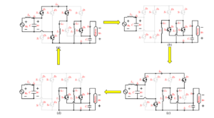
Taking the charging state as an example, the operation of the presented converter topology is shown in Figure 2. Assume the duty-cycle d1 is less than 0.5 and the grid voltage ug is greater than zero, the operation mode is shown as above [1] [4].
State 1 (t1–t2): from Figure 2a, S5 , S8 are on, S6 , S7 are off. The voltage across inductor L1 is expressed as: u L1 = | ug |.uL1 is positive, increasing linearly with a slope of (| ug |)/L. And the energy is transferred from the grid to the inductor L1. The voltage across inductor L2 is expressed as: u L2 = −ub, uL2 is negative, iL2 decreases linearly with a slope of (ub )/L. The energy stored in the inductor L2 is transferred to the battery.
State 2 (t2–t3): from Figure 2b, S6, S8 are on and S5, S7 are off. The energy in the inductors L1, L2 is transferred to the battery through S6 and S8. During this interval, the two inductor currents i L1 and iL2 decrease linearly with a slope of ( ub )/L.
State 3 (t3–t4): from Figure 2c, S6 , S7 are on and S5 , S8 are off. u L2 is positive and the energy is transferred from the grid to the inductor L2 . u L1 is negative and the energy stored in the inductor L1 is transferred to the battery.
State 4 (t4–t5): from Figure 2d, S6 , S8 are on and S5 , S7 are off. This state is the same as state 2, so the energy in the inductors L1 , L2 is transferred to the battery through S6 and S8 .
In addition, the converter is able to work in other modes, and the similar analysis method can be applied. Therefore, due to space limits, the details are neglected here.
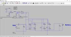
Interpretation of circuit design and Simulation results:
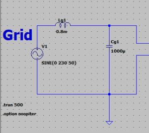
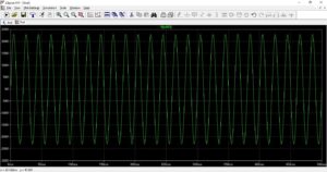
Figure 3 represents the Grid side is AC input 0 to 230 volts and 50 Hz frequency. The LC (Lg1= 0.8mH, Cg1= 1000uF) input filter is used to prevent the high-frequency harmonic currents generated by the converter from flowing into grid. .train 500 means the simulation time of LTSpice is 500ms.
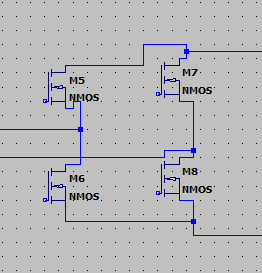
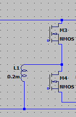
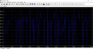
Figure 4 represents the full-bridge converter is used to rectify the AC input voltage to a DC voltage or invert the DC voltage to an AC voltage. Moreover, the bidirectional power flow is achieved. To improve the converter efficiency, the switches of the full-bridge converter commutate at the line frequency.
Full Bridge AC to DC Converter:
- Rectification (AC to DC):
- The Full Bridge Converter is a configuration of power electronics switches (transistors or thyristors) arranged in a bridge topology.
- During the positive half-cycle of the AC input voltage, two diagonally opposite switches are turned on, allowing current to flow through the load. This process repeats during the negative half-cycle using the other pair of switches.
- The result is a pulsating DC voltage across the load.
2. Bidirectional Power Flow:
- The Full Bridge Converter, by its nature, allows bidirectional power flow. It can not only convert AC to DC but can also invert DC to AC.
- This bidirectional capability is crucial for applications like electric vehicle charging, where power needs to flow both ways – from the grid to the battery during charging and from the battery to the grid during vehicle-to-grid (V2G) scenarios.
3. Commutation at Line Frequency:
- To improve efficiency, the switches of the Full Bridge Converter are typically designed to commutate or switch at the line frequency. This synchronization helps minimize switching losses.
4. PWM controller Circuit:
Figure 5 shows the 50% duty cycle means that the pulse is ON for half of the total cycle time. Now, let’s look at the components in the control circuit:
You can download the Project files here: Download files now. (You must be logged in).
- Op-amp (Operational Amplifier): It’s probably being used as a comparator in this context. The op-amp compares a reference voltage with a triangular waveform (commonly used in PWM circuits) to generate the PWM signal.
- OR gate: This gate is likely used to combine signals. In PWM circuits, it might be used to combine the output of the op-amp with another signal, perhaps a feedback signal or an external control signal.
- SR latch (Set-Reset latch): This is a type of digital circuit that has two inputs (Set and Reset) and two outputs (Q and ~Q). The outputs hold the state of the latch based on the inputs. It can be used to store binary information.
- NMOS gate driver: This is probably used to drive the gate of an NMOS (N-channel Metal-Oxide-Semiconductor) transistor. NMOS transistors are often used in electronic circuits.
In LTSpice, these components are likely part of a simulation setup to model and analyze the behavior of your PWM control circuit with a 50% duty cycle. The op-amp generates the PWM signal, the OR gate combines signals, and the SR latch might be involved in the memory or feedback aspect of your circuit. The NMOS gate driver is responsible for driving the NMOS transistor.
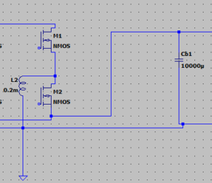
Full Bridge DC to AC Converter:
Inversion (DC to AC):
- In DC to AC mode, the Full Bridge Converter operates differently. It takes a DC voltage (often from a battery) and converts it into an AC voltage.
- This is achieved by switching the transistors or thyristors in a specific sequence. By turning on and off the switches in a controlled manner, the converter creates an AC waveform.
Bidirectional Power Flow:
- The bidirectional capability is again evident here. The same Full Bridge Converter can handle power flow in both directions. When used in an electric vehicle, it can draw power from the battery to supply the AC motor, and it can also push power back to the grid during V2G scenarios.
Synchronization and Control:
- The control system plays a crucial role in determining the output waveform’s frequency, magnitude, and phase. Synchronization with the grid is essential to ensure the output is in phase with the grid voltage during DC to AC conversion.
Boost converter which increase the voltage level from 230 to 400 after converting the DC to DC. Then this 400 DC voltage charges the EV battery. In Figure 8, a Boost converter is depicted, designed for AC to DC step-up conversion. This converter effectively elevates the voltage level from 230 volts to 400 volts by converting the AC input to DC. The resulting 400-volt DC output is then employed to charge the electric vehicle (EV) battery. This boost conversion process is instrumental in efficiently transforming the incoming AC power to a higher voltage, facilitating optimal charging of the EV battery with the elevated voltage output.
Buck converter which reduce the voltage level from 400 to 230 DC from battery. Then this voltage goes to the bridge rectifier and again converted into AC. Hence battery will provide the backup of EV to grid side. In Figure 9, a Buck converter is illustrated, serving to decrease the voltage level from 400 volts to 230 volts DC, drawing power from the battery. Subsequently, this reduced voltage is directed to a bridge rectifier, where it undergoes conversion back into AC. This cyclic process enables the battery to function as a backup for the electric vehicle (EV) in supplying power to the grid, showcasing the versatile bidirectional capability of the system. The Buck converter’s role in voltage reduction ensures compatibility with the grid’s voltage requirements, allowing seamless energy transfer between the EV and the grid during backup operations.
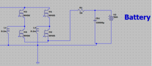
In Figure 10, the power factor correction (PFC) is achieved using the output capacitor Cb1 in conjunction with the interleaved parallel bidirectional buck-boost DC/DC converter. This converter not only minimizes battery current ripple but also enhances the overall quality of input current. The utilization of this topology allows for effective power factor correction, ensuring that the current drawn from the power source aligns with the voltage waveform, optimizing efficiency and reducing harmonic distortions [2]. Consequently, the incorporation of Cb1 and the interleaved converter in this setup not only improves battery performance but also enhances the converter’s capability to operate with high input current quality, contributing to a more efficient and stable power transfer system. The interleaved parallel bidirectional buck-boost DC/DC converter is employed to reduce the battery current ripple. Additionally, power factor correction (PFC) and high input current quality can be realized with the topology.
Output Results
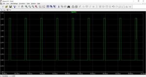
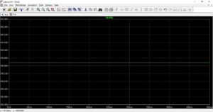
In Figure 13, the depicted DC output voltage represents the post-rectification stage, referred to as “noisy DC output voltage,” fluctuating between 397 and 398.5 volts. This variation in voltage levels suggests a certain degree of noise or ripple in the rectified DC output [3]. The term “noisy” indicates that the voltage exhibits slight fluctuations within this range, potentially influenced by factors such as transient effects, switching dynamics, or other sources of electrical interference. Analyzing and understanding these voltage variations is crucial for assessing the stability and quality of the rectified output, as well as for implementing any necessary filtering or control mechanisms to mitigate the observed noise.
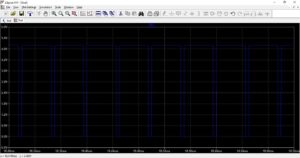
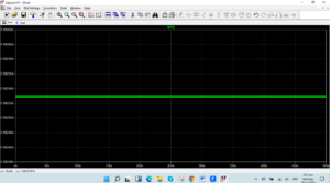
In Figure 14, the illustration portrays the DC output as a “smooth voltage,” maintaining a constant level of 398.84 volts DC. This indicates a stabilized and regulated DC output, specifically tailored for charging the battery. The term “smooth” suggests a reduced presence of voltage variations or ripple, reflecting an optimized and consistent power supply. This stable voltage output is crucial for efficient and reliable charging of the battery, ensuring a steady and controlled energy flow without the fluctuations observed in the earlier rectified output.

In Figure 15, the illustration showcases the “Pure DC output voltage” emanating from the electric vehicle (EV) bidirectional charger designed for a 400 DC volt battery. This depiction implies that the output voltage has undergone a refinement process, likely involving filtering or smoothing mechanisms, resulting in a stable and consistent DC voltage without the fluctuations or noise observed in earlier stages [4] [5]. This purified DC output, specifically tailored for a 400-volt battery, signifies the readiness of the charger to deliver a reliable and regulated voltage suitable for efficiently charging the EV battery, emphasizing the importance of achieving a consistent and clean power supply in the charging process.
In Figure 16, the illustration showcases the measured current, denoted as I=7.98253A, flowing through the resistor R1 in the Bidirectional Electric Vehicle (EV) charger circuit. This current measurement is a crucial parameter for assessing the performance and efficiency of the charger circuit, providing valuable insights into the electrical characteristics of the system. Monitoring the current through R1 allows for a detailed analysis of the charging process, aiding in the optimization and refinement of the bidirectional EV charger’s design. The specific value of 7.98253A indicates the magnitude of the current at the measured instance, serving as a key metric for further evaluation and potential adjustments to enhance the overall functionality of the charging system.
| Table 1: Simulation parameters | |
| Parameters | Values
|
| Input Grid Voltage V1 | 230 V |
| Input filter inductance (Lg) | 0.8mH |
| Input filter capacitor (Cg1) | 1000uF |
| DC inductor L1 | 0.2mH |
| DC inductor L2 | 0.2mH |
| Output filter capacitor (Co ) | 10^3 uF |
| Switching frequency (fs ) | 20KHz |
| Battery voltage (V2 ) | 400V |
Table values for the circuit of EV charger
In the simulation, various parameters, as detailed in Table 1, have been employed to characterize and evaluate the performance of the system. A crucial consideration in the simulation is the selection of a switching frequency of 20 kHz. This choice represents a deliberate trade-off between Total Harmonic Distortion (THD) and the overall efficiency of the converter. Additionally, an input filter has been integrated into the design to mitigate the risk of overvoltage and minimize distortion in the input current. This input filter plays a key role in enhancing the stability and reliability of the system during operation.
Moreover, the DC inductors, denoted as L1 and L2, are designed to operate within the linear range of the flux density-magnetic field strength (B-H) curve. This ensures that the inductors perform optimally and reliably, contributing to the efficiency of the overall system [5]. The loads in this simulation are represented by 38 Ah-capacity lead-acid batteries, each with a nominal voltage of 400 V. These battery characteristics are essential factors as they directly influence the charging and discharging dynamics within the bidirectional converter, impacting the overall performance and energy transfer efficiency of the simulated system.
You can download the Project files here: Download files now. (You must be logged in).
Converters advantages and disadvantages and how to use it in different applications
Advantages of Bidirectional Converters in EVs:
- Regenerative Braking: Bidirectional converters allow the conversion of kinetic energy during braking back into electrical energy. This energy can be fed back into the battery, improving overall efficiency.
- Energy Management: These converters enable effective energy management, allowing the transfer of power bidirectionally between the battery and other components such as the motor or the grid. This enhances the flexibility of energy flow within the system.
- Grid-to-Vehicle (G2V) and Vehicle-to-Grid (V2G) Capabilities: Bidirectional converters enable not only charging the EV from the grid (G2V) but also discharging energy back to the grid (V2G). This bidirectional capability supports grid stabilization and provides an opportunity for the EV owner to contribute excess energy back to the grid.
- Optimized Battery Charging and Discharging: Bidirectional converters facilitate controlled and optimized charging and discharging of the battery. This is crucial for extending battery life and ensuring efficient use of stored energy.
- Emergency Power Supply: In case of power outages or emergencies, bidirectional converters can be used to supply power from the EV battery to critical loads, acting as a mobile power source.
Disadvantages of Bidirectional Converters in EVs:
- Complexity and Cost: Implementing bidirectional converters adds complexity to the EV power electronics system, which may increase the overall cost and maintenance requirements.
- Efficiency Losses: Bidirectional energy flow introduces additional conversion stages, leading to some energy losses during power transfer. The efficiency of bidirectional converters is a critical factor to consider.
- Control Challenges: Managing bidirectional power flow requires sophisticated control algorithms to ensure safe and efficient operation. This complexity can lead to challenges in control system design and implementation.
Applications of Bidirectional Converters in EVs:
- Vehicle-to-Grid (V2G): Bidirectional converters play a crucial role in V2G applications, where the EV can act as a distributed energy resource, feeding power back to the grid during peak demand or emergencies [6].
- Energy Storage Systems (ESS): Bidirectional converters are used in conjunction with energy storage systems to efficiently manage the charging and discharging of batteries, supporting renewable energy integration and grid stability.
- Regenerative Braking Systems: Bidirectional converters capture and transfer energy during braking, improving overall efficiency and reducing wear on traditional braking systems [7].
- Emergency Power Supply: Bidirectional converters can be utilized to provide emergency power for residential or commercial applications during grid outages, showcasing the versatility of EVs as mobile power sources.
You can download the Project files here: Download files now. (You must be logged in).
Conclusion
In the scope of this project, a single-phase bidirectional AC/DC converter designed for Vehicle-to-Grid (V2G) applications has been introduced. This innovative topology comprises a line frequency-commutated unfolding bridge paired with an interleaved buck-boost stage. Operating in a buck-boost charging/discharging mode, the converter accommodates various battery types by providing different voltage levels. The analysis of the charger’s operational principle demonstrates its ability to support and exchange reactive power with the grid, marking it as a valuable bidirectional charging solution [8]. Notably, the charger exhibits appealing features such as bidirectional power flow, minimal current ripple, and a broad battery voltage range, making it well-suited for V2G applications. Simulation and experimental results have been presented, affirming the efficacy and viability of this bidirectional charger in practical V2G scenarios. This project’s emphasis on bidirectional power flow, low current ripple, and adaptability to diverse battery voltages positions the presented charger as a robust contender for V2G applications [9] [10]. The successful validation through simulations and experiments underscores its potential contribution to enhancing the efficiency and versatility of electric vehicle charging systems in real-world, grid-interconnected environments.
References
- Jin, X. Zhang, Y. Tang, and Y. W. Li, “A Single-Phase Bidirectional AC-DC Converter With Power Factor Correction and Fast Regulation,” IEEE Transactions on Power Electronics, vol. 28, no. 4, pp. 1711–1722, Apr. 2013, doi: 10.1109/TPEL.2012.2209962.
- S. Masoum, P. S. Moses, and M. A. Masoum, “Optimal Charging of Plug-In Electric Vehicles in Smart Grids Considering Dynamic Energy Prices and V2G Services,” IEEE Transactions on Smart Grid, vol. 5, no. 1, pp. 511–518, Jan. 2014, doi: 10.1109/TSG.2013.2268864.
- Kanchev, D. Lu, F. Colas, V. Lazarov, and B. Francois, “Energy Management and Operational Planning of a Microgrid With a PV-Based Active Generator for Smart Grid Applications,” IEEE Transactions on Industrial Electronics, vol. 58, no. 10, pp. 4583–4592, Oct. 2011, doi: 10.1109/TIE.2011.2107716.
- Yang, K. Zhou, and B. Liu, “Review on Electric Vehicle Bidirectional Charger for V2G Applications—Current Status and Challenges,” Journal of Modern Power Systems and Clean Energy, vol. 8, no. 1, pp. 1–15, Jan. 2020, doi: 10.35833/MPCE.2019.000256.
- Wang and J. Wang, “Self-Healing Resilient Distribution Systems Based on Sectionalization Into Microgrids,” IEEE Transactions on Power Systems, vol. 30, no. 6, pp. 3139–3149, Nov. 2015, doi: 10.1109/TPWRS.2014.2365703.
- Yilmaz and P. T. Krein, “Review of Battery Charger Topologies, Charging Power Levels, and Infrastructure for Plug-In Electric and Hybrid Vehicles,” IEEE Transactions on Power Electronics, vol. 28, no. 5, pp. 2151–2169, May 2013, doi: 10.1109/TPEL.2012.2212917.
- Ghosh and G. Narayanan, “A Single-Phase Soft-Switched High-Frequency AC Link Inverter,” IEEE Transactions on Industrial Electronics, vol. 57, no. 2, pp. 735–743, Feb. 2010, doi: 10.1109/TIE.2009.2028430.
- He and Y. W. Li, “An Enhanced Microgrid Load Demand Sharing Strategy,” IEEE Transactions on Power Electronics, vol. 27, no. 9, pp. 3984–3995, Sep. 2012, doi: 10.1109/TPEL.2012.2188876.
- Vazquez, S. M. Lukic, E. Galvan, L. G. Franquelo, and J. M. Carrasco, “Energy Storage Systems for Transport and Grid Applications,” IEEE Transactions on Industrial Electronics, vol. 57, no. 12, pp. 3881–3895, Dec. 2010, doi: 10.1109/TIE.2010.2076414.
- Khaligh and S. Dusmez, “Comprehensive Topological Analysis of Conductive and Inductive Charging Solutions for Plug-In Electric Vehicles,” IEEE Transactions on Vehicular Technology, vol. 61, no. 8, pp. 3475–3489, Oct. 2012, doi: 10.1109/TVT.2012.2207545.
You can download the Project files here: Download files now. (You must be logged in).
Keywords: Bidirectional Single-Phase, EV Charger, LTSpice Simulation, Vehicle-to-Grid (V2G)


Responses